Homework 5 - Sequential
Circuits
CE 433 Embedded Devices
2024 SpringName: Joel Nash
Email:
jxnash@gmail.com
Tasks:
1. In Section
1, don't look at the logic equations provided to you. From the
state table, find the logic equations for q1(n+1) and y and draw
the sequential circuit for q1(n+1) and y. (10 points)
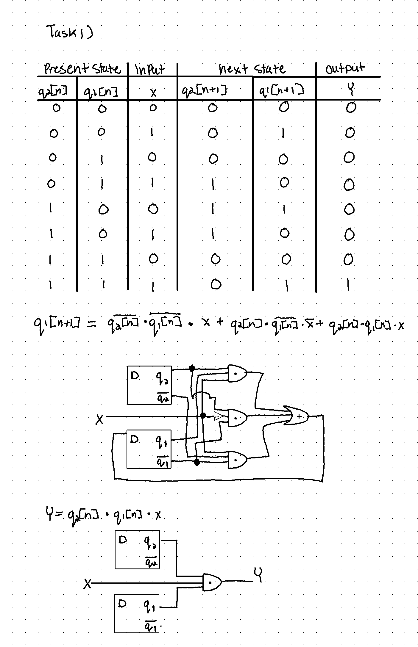
Figure 1: State
table of the circuit, the logic equations of q1[n+1], and Y, and
their resulting sequential circuits.
2. Repeat the
work in Section 3. Use two methods, the given one and the
behavioral one. Show simulation results. (15 points)
Logic
Equations:
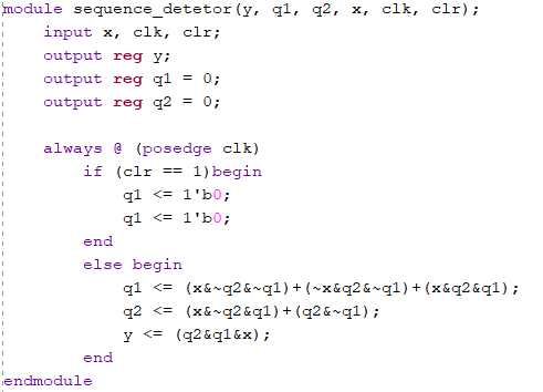
Figure 2: Vivado
code of the logic equations found in the first part of task 1, a
sequence decoder looking for a specific logic output, (aka. y).
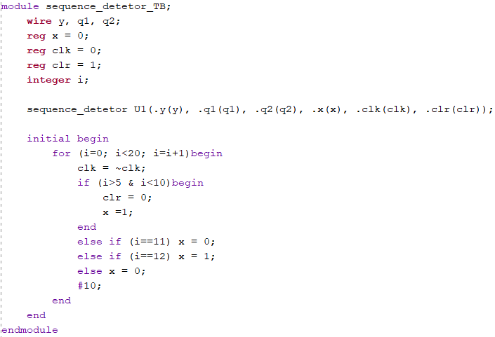
Figure 3: Vivado
code of the sequence decoder test-bench, going through different
logic inputs to see the result 'y'.
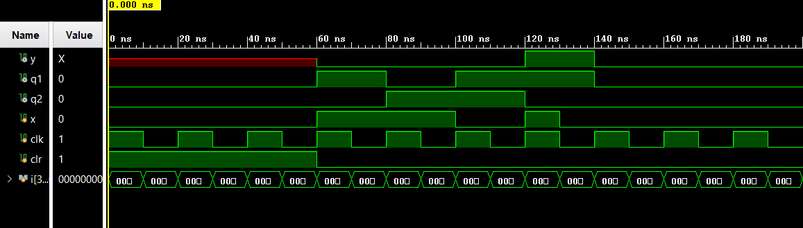
Figure 4:
Simulation of the the logic equations in the sequence decoder
program.
Behavioral:
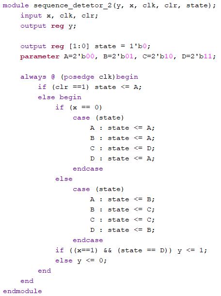
Figure 5: Vivado
code of the sequence decoder using the behavior method instead of
the logic equations.
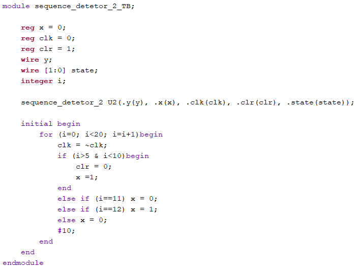
Figure 6: Vivado
code for the behavioral sequence decoder test-bench, changing the
inputs for show the logic just like the logic equations sequence
decoder test-bench.

Figure 7:
Simulation of the behavior sequence decoder, this should/is the
same result as using the logic equations.
3. Similar to
the sequence detector in Section 3, change the sequence to be
detected to 1011, design the state diagram, draw the truth
table, find the logic equations, and design the verilog module
and test-bench to verify the logic. (15 points)
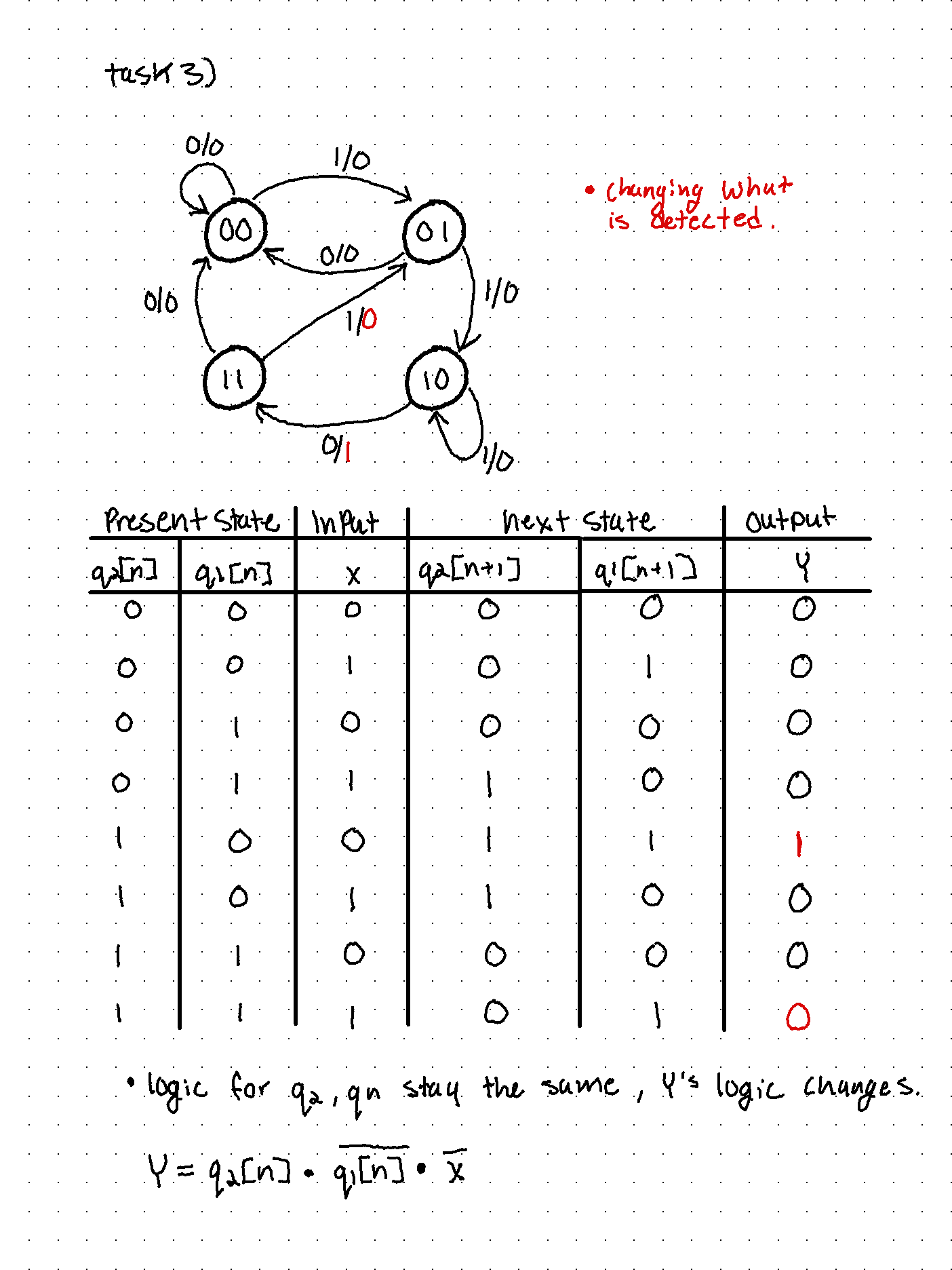
Figure 8: Image
showing the changes made to the state diagram and the state table,
and then the new equation for 'y', that the sequence decode is
detecting a new change in the state, from 10 -> 11.
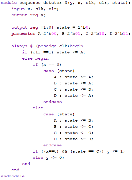
Figure 9: Vivado
code for the new sequence decoder using the behavior method, that
is detecting a different set of inputs.
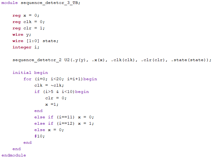
Figure 10: Vivado code of the test-bench for the new sequence decoder.
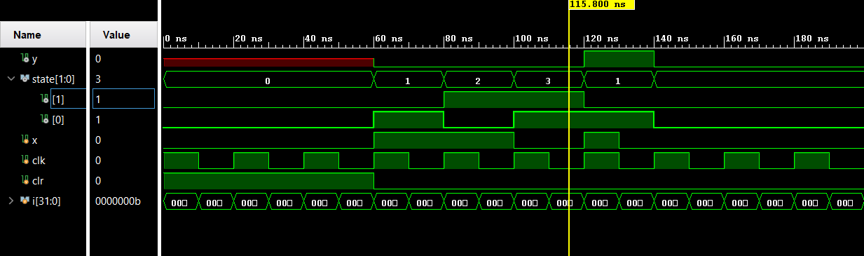
Figure 11:
Simulation results of the sequence decoder looking at a different
input set state change, (aka. 10->11).
4. Simulate
the four types of shift registers in Section 5. (20 points)
SISO:
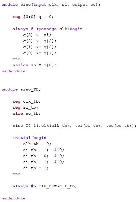
Figure 12:
Vivado code of serial-in serial-out shift register operation,
taking in a input in 1-bit chunks and shifting them through a temp
variable to shift back out in 1-bit chunks.
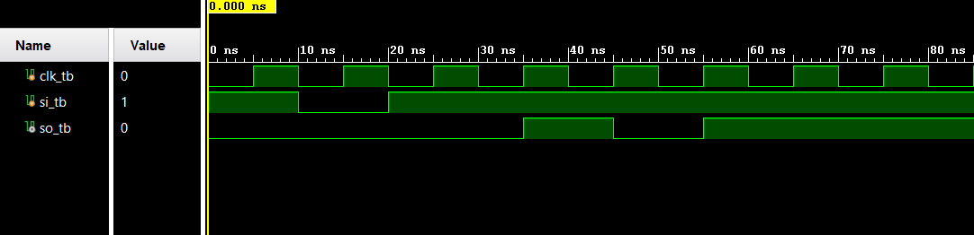
Figure 13:
Simulation of the serial-in serial-out function
PISO:
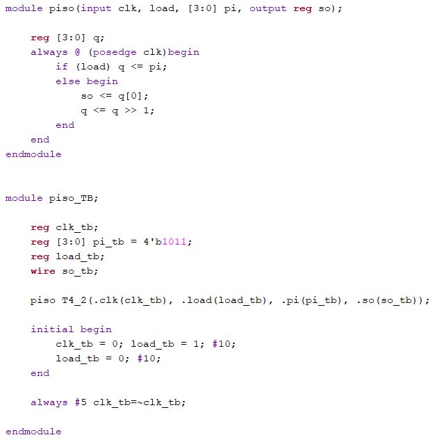
Figure 14: Vivado code of parallel-in serial-out shift
register operation, taking in a 4-bit input and shifting them
through a temp variable to shift out in 1-bit chunks.
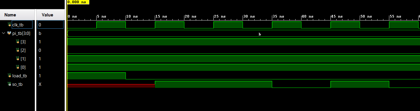
Figure 15: Simulation of the parallel-in serial-out
function
PIPO:
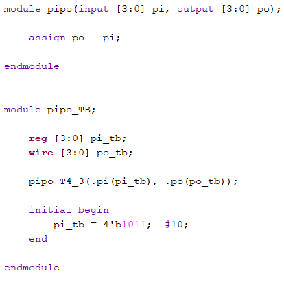
Figure 16: Vivado code of parallel-in parallel-out
shift register operation, taking in a 4-bit input and shifting out
in a 4-bit output.
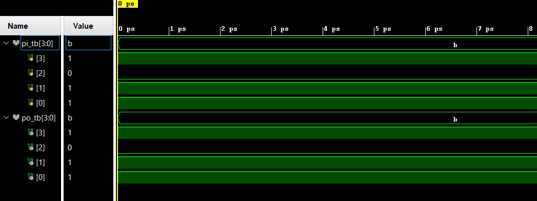
Figure 17: Simulation of the parallel-in parallel-out
function
SIPO:
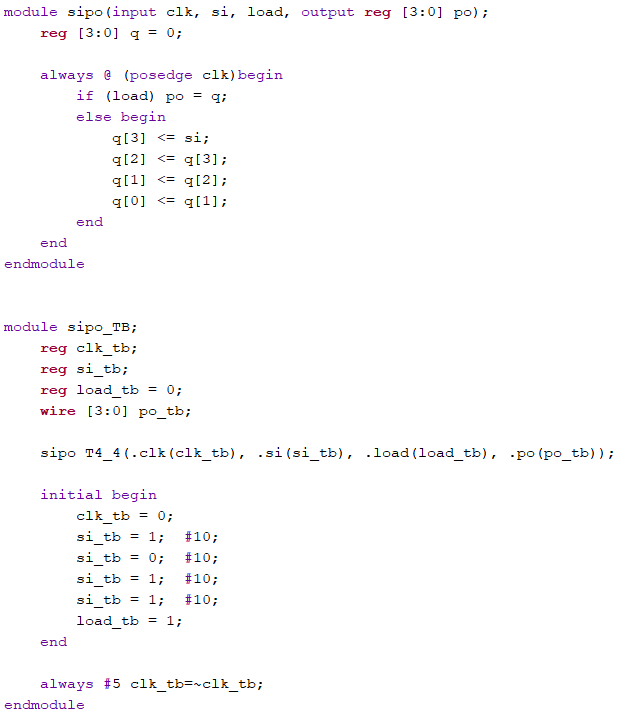
Figure 18: Vivado code of serial-in serial-out shift
register operation, taking in an input in 1-bit chunks and
shifting them into a temp variable to shift out in a 4-bit
parallel chunk.
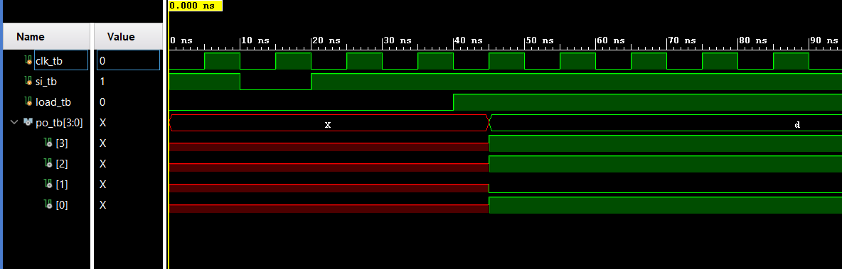
Figure 19: Simulation of the serial-in parallel-out
function
5. Build a
counter module and show the simulation results. (20 points)
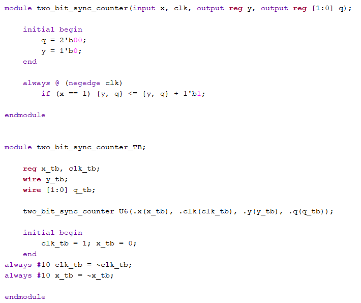
Figure 20:
Vivado code of a two bit synchronous up counter module.

Figure 21:
Simulation of the two bit counter.
6. Find the
logic equation of the following circuit and implement it in
verilog. Show the simulation results. (20 points)
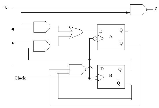
Figure 22:
Circuit diagram that is used to find the logic equations.
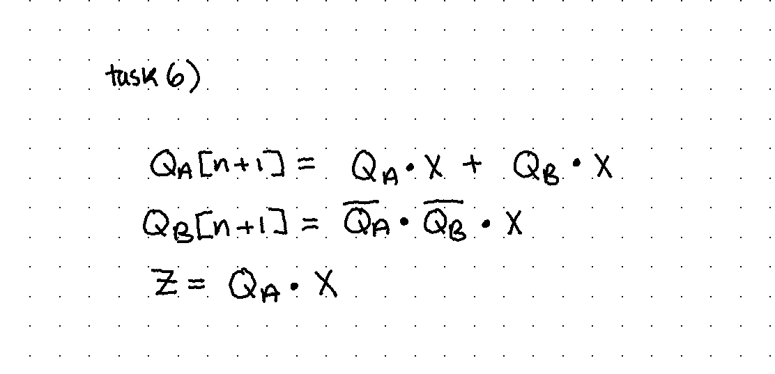
Figure 23: The
resulting logic equations found from the logic diagram.
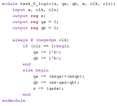
Figure 24: Vivado code for the logic equations found from the logic diagram, coded using just the logic equations.
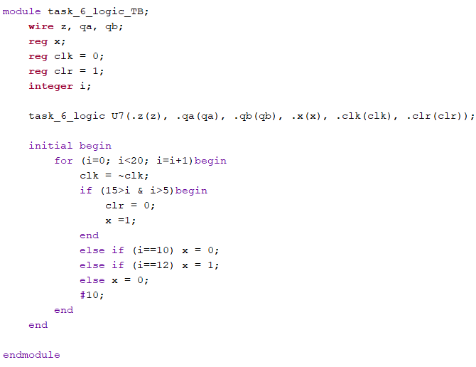
Figure 25:
Vivado code of the test-bench, for the logic equations found,
cycling the input to show the results.
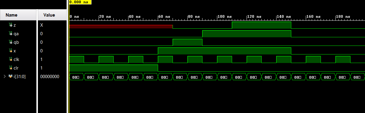
Figure 26:
Simulation results of the logic test-bench.