Homework 4 - Data Storage
Units
CE 433 Embedded Devices
2024 SpringTasks:
1. Repeat the simulation in
Sections 1 - 3. (20 points)
Section 1: SR latch / flip flop
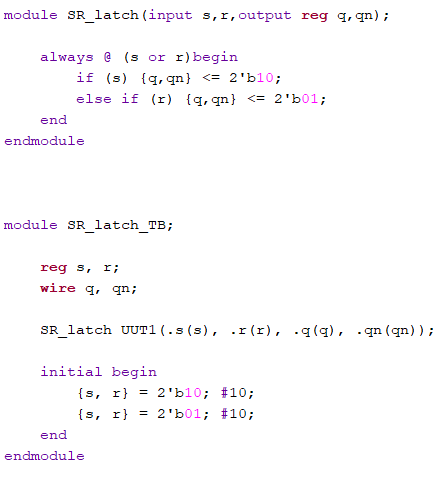
Figure 1: Vivado code of the SR latch.
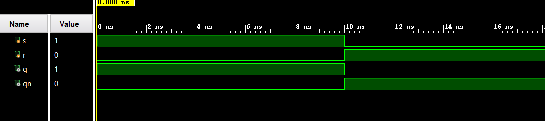
Figure 2: Simulation of the SR latch.
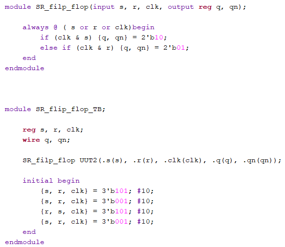
Figure 3: Vivado code for a SR control Latch.
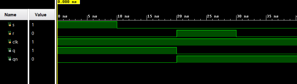
Figure 4: Simulation of the SR control
latch.
Section 2: D latch / flip flop
level triggered
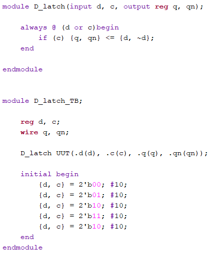
Figure 5: Vivado code of a D latch,
and the code for the D latch test-bench.
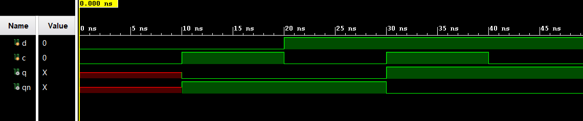
Figure 6: Simulation of the D latch,
demonstrates the logic of changing the inputs 'd' and 'c', and
how the input input 'c' sets the outputs 'q' and 'qn' to 'd' and
'~d' respectfully.
Section 3: D flip flop
edge triggered
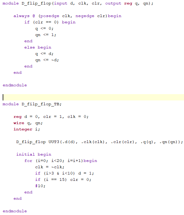
Figure 7: Vivado code for the D flip
flop and the test-bench for the D flip flop. With this you can
see that we still use the D latch logic while introducing the
clock into the mix.
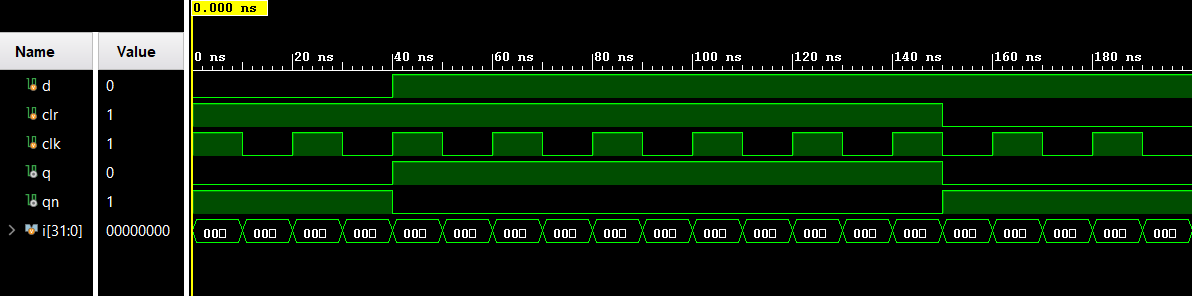
Figure 8: Simulation of the D flip
flop, showing the results from the test-bench. How the inputs
'd', 'clr' and 'clk', effect the outputs 'q' and 'qn'.
2. Build a debounce circuit on a breadboard using a push-button, a passive low-pass filter, and a schmitt trigger IC chip (20 points).
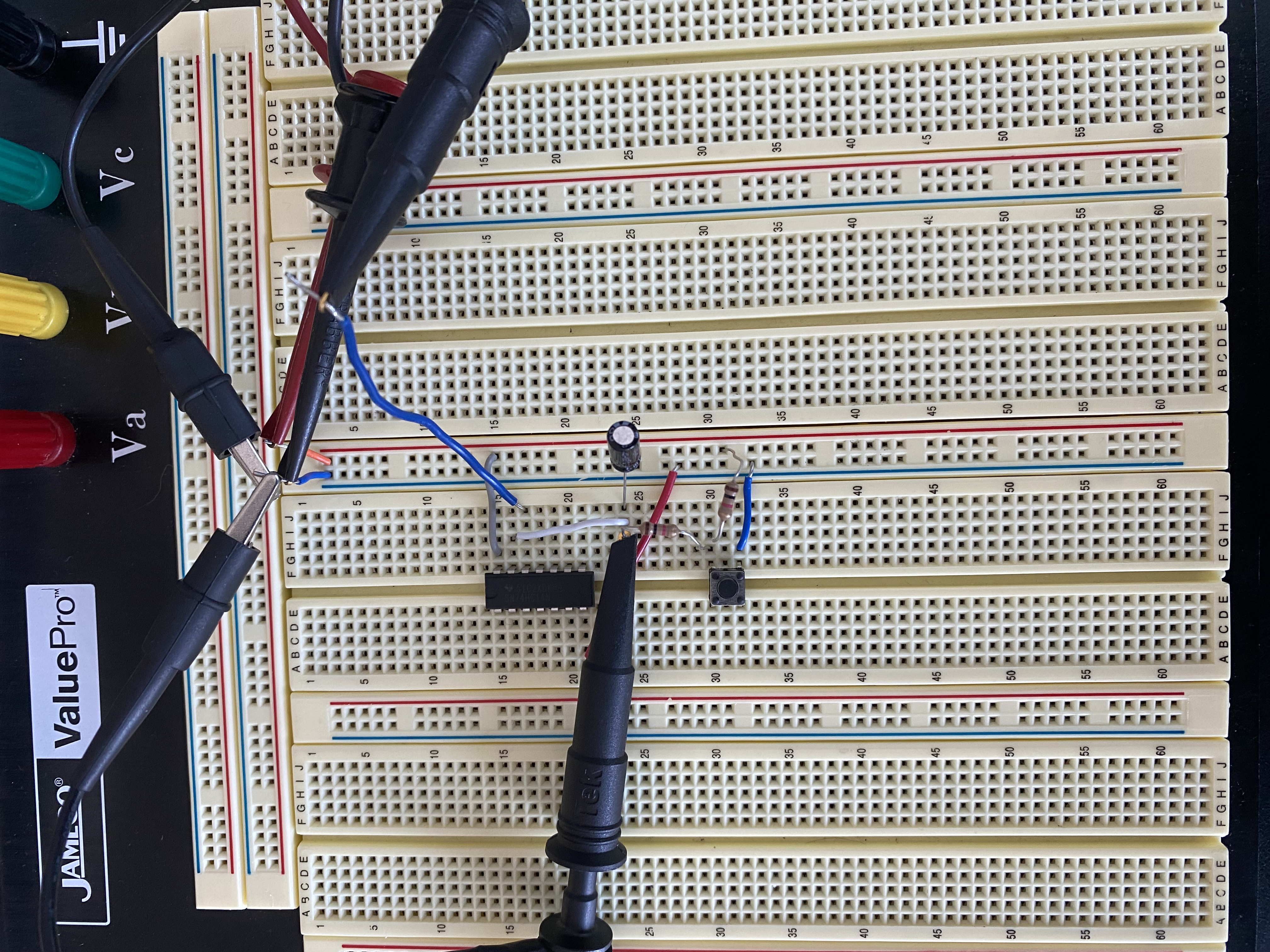
Figure 9: This is a Debounce circuit
built on a breadboard, with a push button.
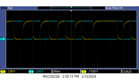
Figure 10: Oscilloscope of the
debounce circuit.
3. Write the test-benches and run
simulations for Section 4 and Section 5. (20 points)
Section 4: JK Flip-Flop
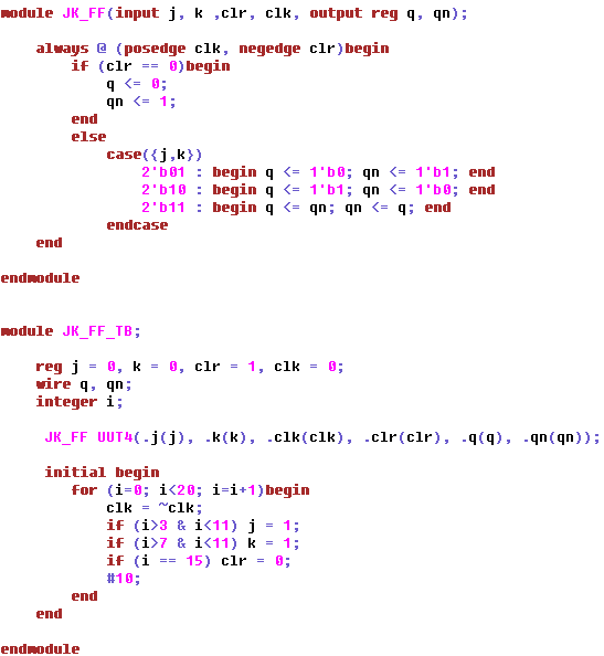
Figure 11: Vivado code (in vim) of the JK Flip-Flop and the corresponding test-bench. This has 'j', 'k' and the clock as inputs, 'q', 'qn' as outputs. there are four different types of logical outputs: '1', '0', no-change, and toggle. In this the inputs are being changed to show this logic.
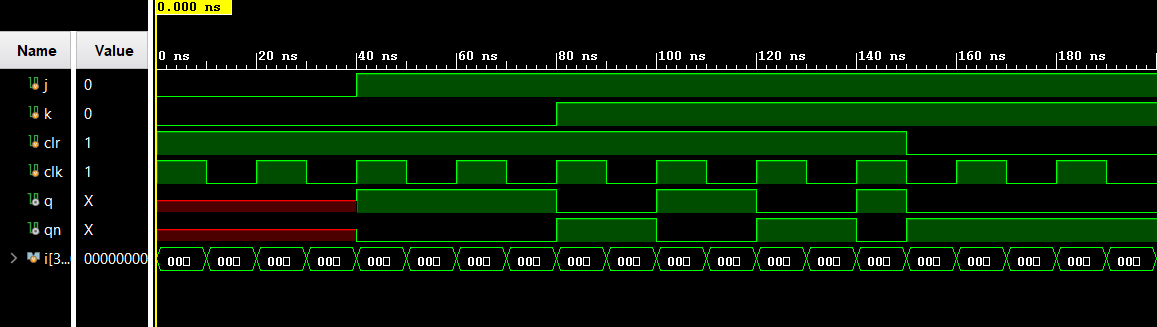
Figure 12: Simulation of the JK Flip-Flop.
Section 5: T Flip-Flop
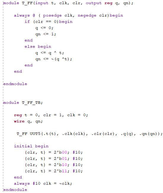
Figure 13: Vivado code of the T Flip-Flop, and it's test-bench. The T Flip-Flop is similar to the JK Flip-Flop, but only uses the toggle function of the JK Flip-Flop.
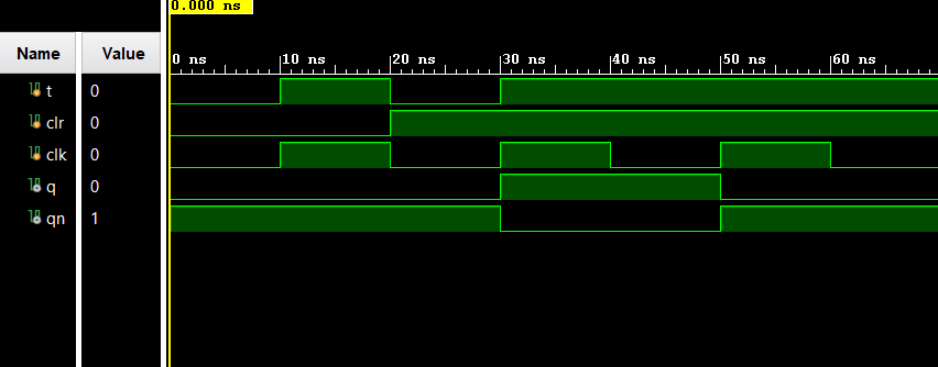
Figure 14: Simulation of the T
Flip-Flop.
4. Repeat all the work in Section 8 and complete the task described in the end of Section 8. (40 points)
In this task we are reading
information from a memory file, and using locations just for
that, using Read Only Memory (ROM). We demonstrate reading in
different types of information, and sometimes manipulating them
into a different formats: 8-bit to 8-bit, hex to hex, hex to
binary, 3-bit to 3bit. Finally we extract data from the ROM IP
core.
Section 8: Rom Memory
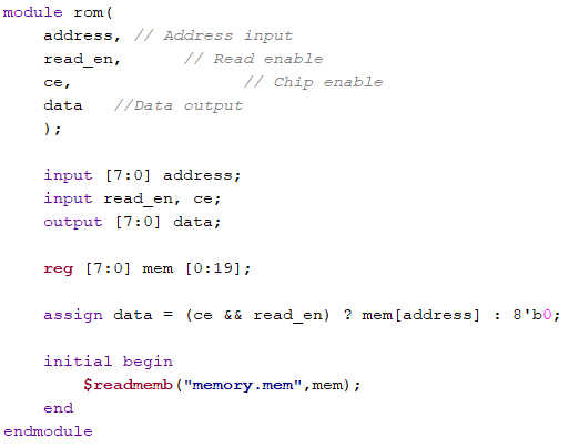
Figure 15: Vivado code for reading
memory from a file, reading a 8-bit binary number and outputting
a 8bit binary number to data.
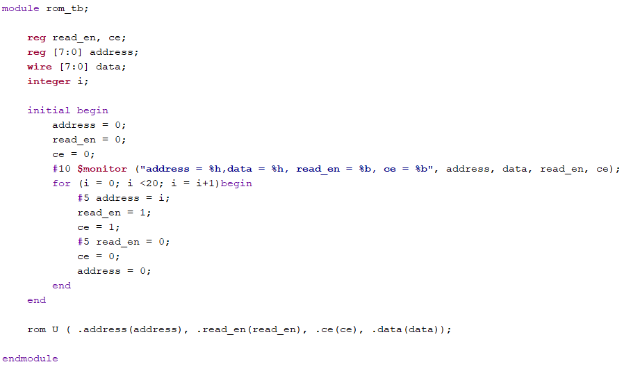
Figure 16: Vivado code of the ROM test-bench.
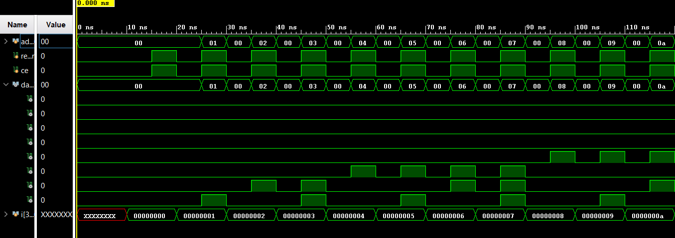
Figure 17: Simulation of the ROM
test-bench reading the information from the memory file.
Section 8:Rom Hex
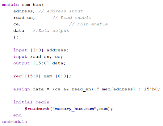
Figure 18:
Vivado code for reading memory from the memory file, reading a
4-digit hex number and outputting a 16bit binary number to data.
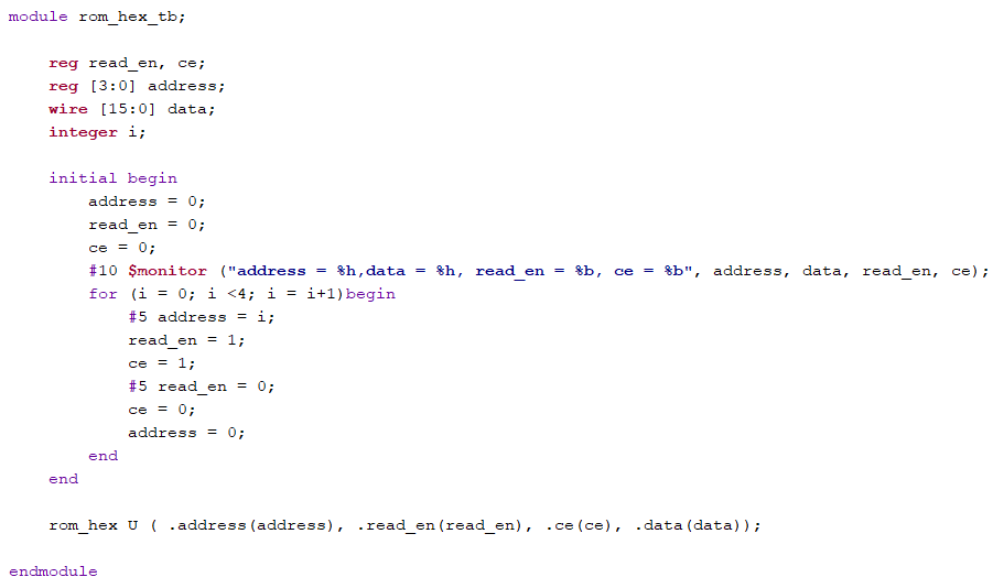
Figure 19:
Vivado code of the test-bench from reading 4 hex to 16bit.
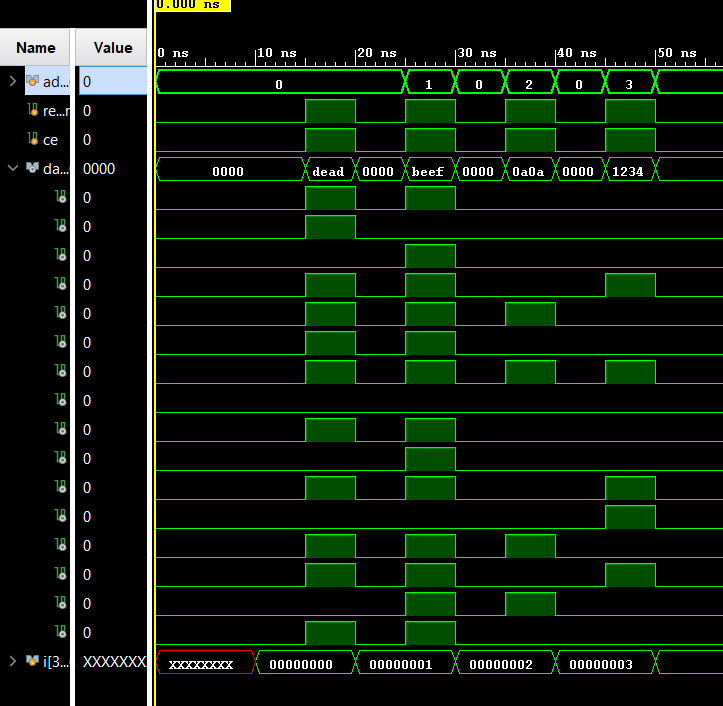
Figure 20: Simulation of the (4-hex to 16bit) ROM test-bench reading the information from the memory file.
Section 8:Rom 2hex(8bit) to
binary(8bit)
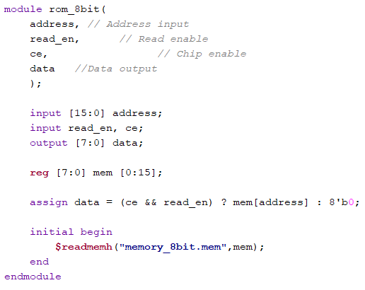
Figure 21:
Vivado code for reading memory from the memory file, reading a
2-digit hex number and outputting a 8bit binary number to data.
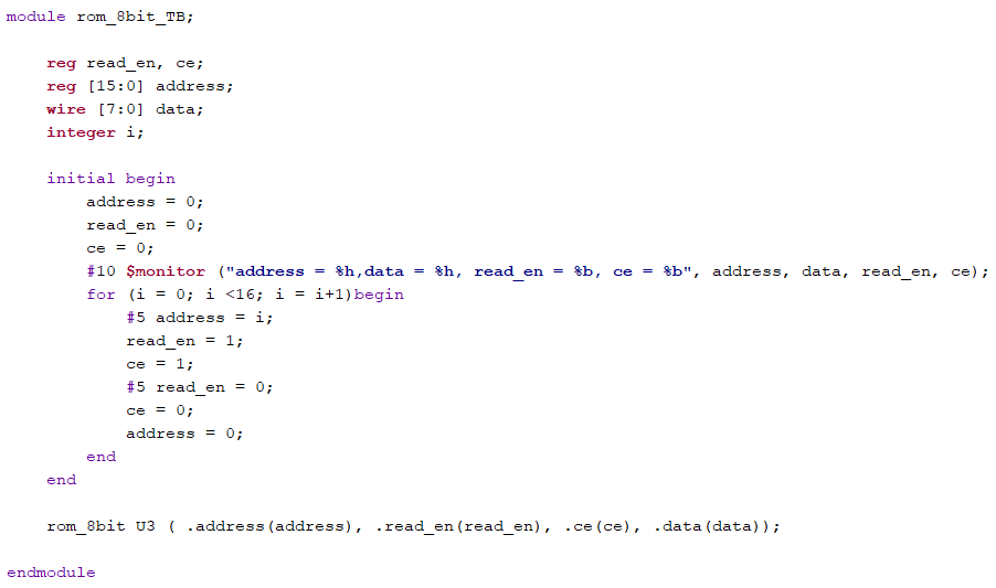
Figure 22: Vivado code of the test-bench from reading 2 hex numbers to 8bit binary number.
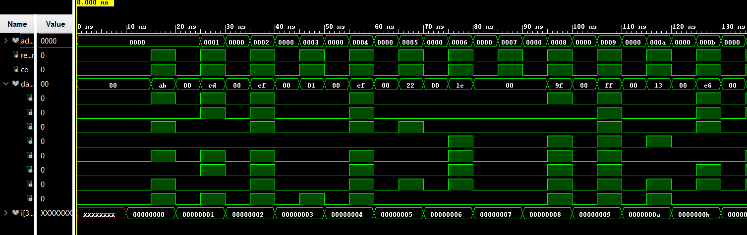
Figure 23: Simulation of the (2 hex numbers
to 8bit binary number) ROM test-bench
reading the information from the memory file.
Section 8:Rom 3-bit binary
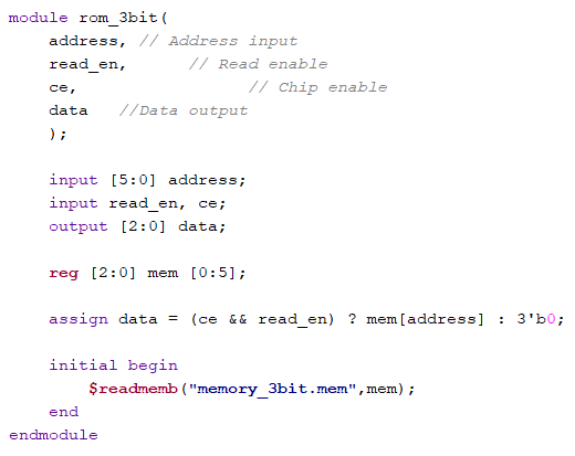
Figure 24:
Vivado code for reading memory from the memory file, reading a
2-digit hex number and outputting a 8bit binary number to data.
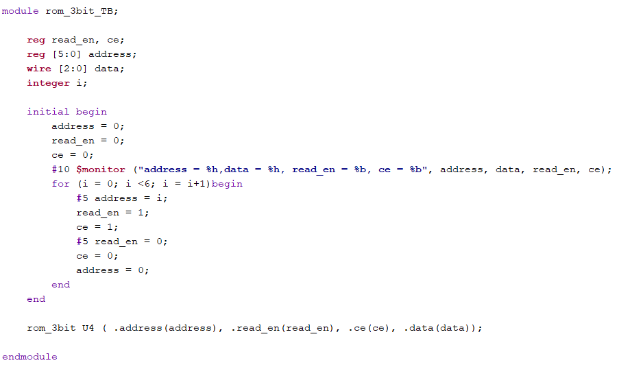
Figure 25: Vivado code of the test-bench from reading 2 hex numbers to 16bit binary number.

Figure 26: Simulation of the (2 hex numbers
to 16bit binary number) ROM test-bench
reading the information from the memory file.
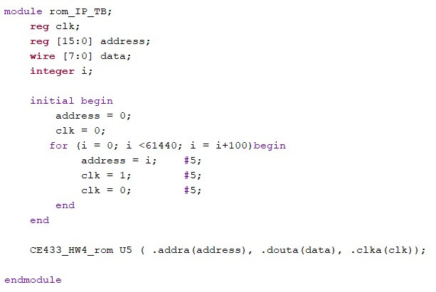
Figure 27:
Vivado code for extracting data from the ROM IP core.
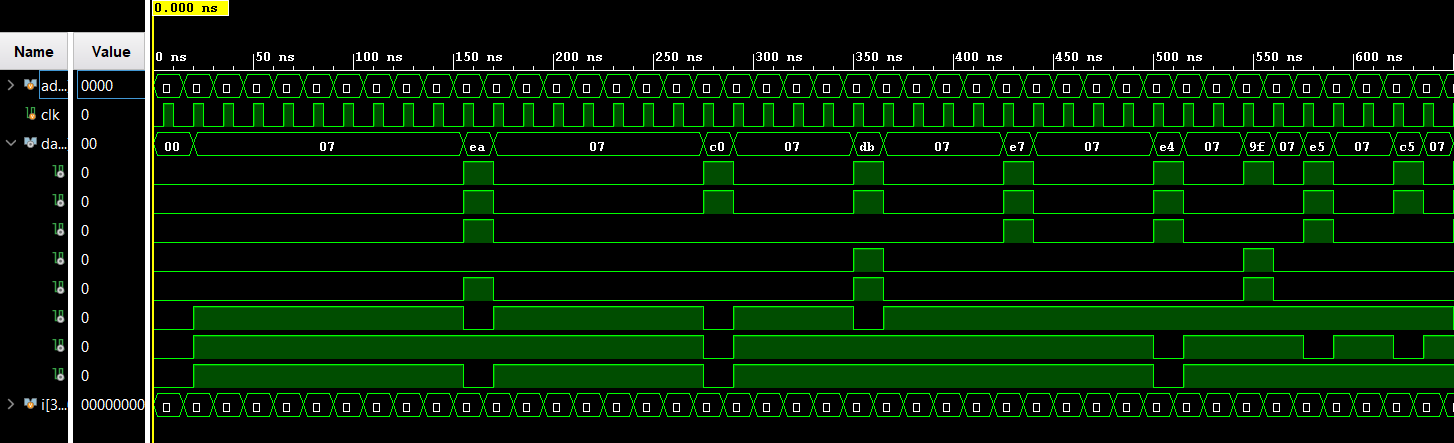
Figure 28: Simulation of the extracting data from the ROM IP core.