Lab 3 - Seven-Segment Display
on an FPGA (2-week lab)
CE 433 Embedded Devices
2024 SpringName: Joel Nash
Email:
jxnash@gmail.com
WEEK 1 Tasks:
Task 1:
Complete the tasks in Sections 1. Show your code, explanation,
and demonstrate it in an embedded video. (20 points)
Using Verilog
and Vivado to demonstrate the following combinational logic blocks
in both simulation and on the board (switches/leds): 1. Inverter,
2. 2-bit full adder, 3. 8-input AND, 4. 4-1 MUX.
Inverter:
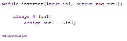
Figure 1: Vivado code for the
inverter function. taking in an input and then outputting the
inverted logic.
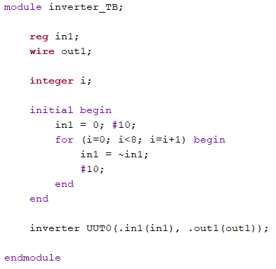
Figure 2: Vivado
code for the inverter test bench. This is using the inverter code
and inputting a variable that changes every 10ns to demonstrate
the logic of the inverter.
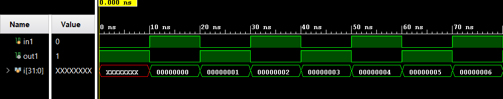
Figure 3:
Simulation results for the inverter test bench, showing the logic
of the input 'in1' and the inverted output 'out1'.
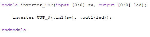
Figure 4: Vivado
code to program the inverter code onto the FPGA board. Using
switches as inputs and outputting to LEDs.
2-bit full adder:
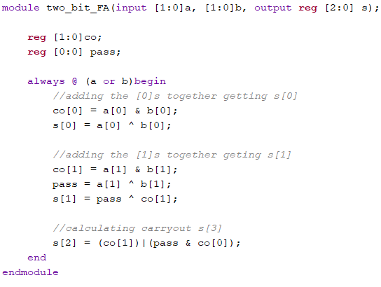
Figure 5: Vivado
code for the 2-bit full adder. This code uses the logic of two
half adders and puts them together to make the 2-bit full adder.
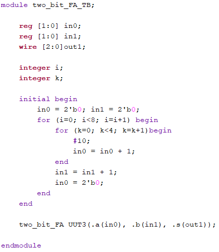
Figure 6: Vivado
code of the 2-bit full adder test bench. Using two inputs and
increment them at different intervals to demonstrate the 2-bit
full adder logic in the resulting simulation.
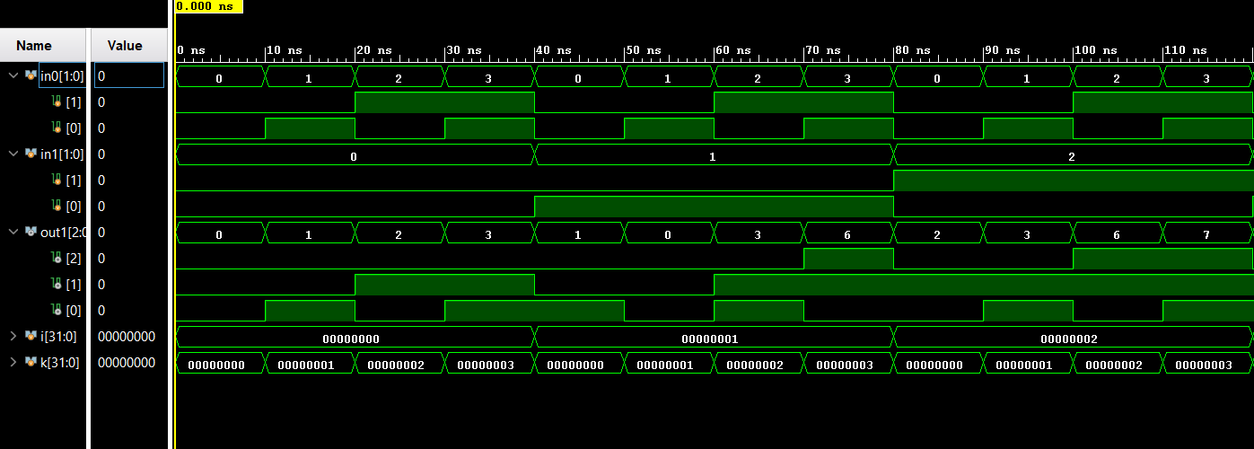
Figure 7:
Simulation of the 2-bit full adder showing the adding of the
inputs 'in0' and 'in1' and the resulting output 'out1' logic.
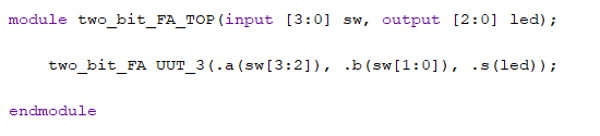
Figure 8: Vivado
code to program the 2-bit full adder onto the FPGA board, using
the switches and LEDs as inputs and outputs.
8-input AND:
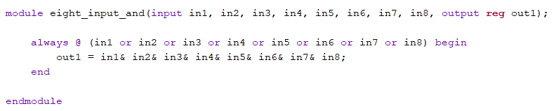
Figure 9: Vivado
code for an 8 input AND gate, taking in eight different inputs and
outputting the AND logic of all eight inputs.
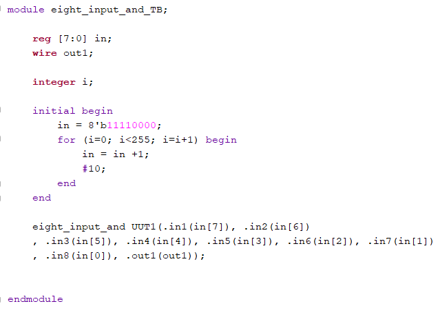
Figure 10:
Vivado code of the 8-input AND gate test bench, taking in a 8-bit
input and using the AND logic on the individual bits to
demonstrate the logic.
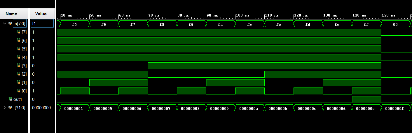
Figure
11: Simulation of the 8-input AND gate. With the 8-bit binary
number being quite large, this snapshot just shows the logic right
before the output equals 1.
Figure 12:
Vivado code to program the FPGA board with the 8-input AND gate
logic, using switches and LEDs as input and outputs.
4-1 MUX:
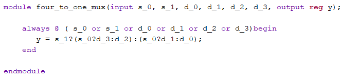
Figure 13:
Vivado code for a four to one multiplexer (aka MUX). This takes in
two sets of inputs 's' and 'd', depending on what state the input
's' is in, the output will change to the corresponding 'd', making
the output 'y' equals a specific 'd'.
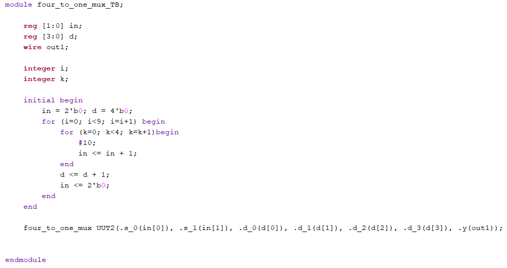
Figure 14:
Vivado code of the four to one MUX test bench to demonstrate the
MUX logic. With this code the two input change at different rates
to show the logic working, for every time the input 'd' is
incremented, the input 's' goes through a full cycle.
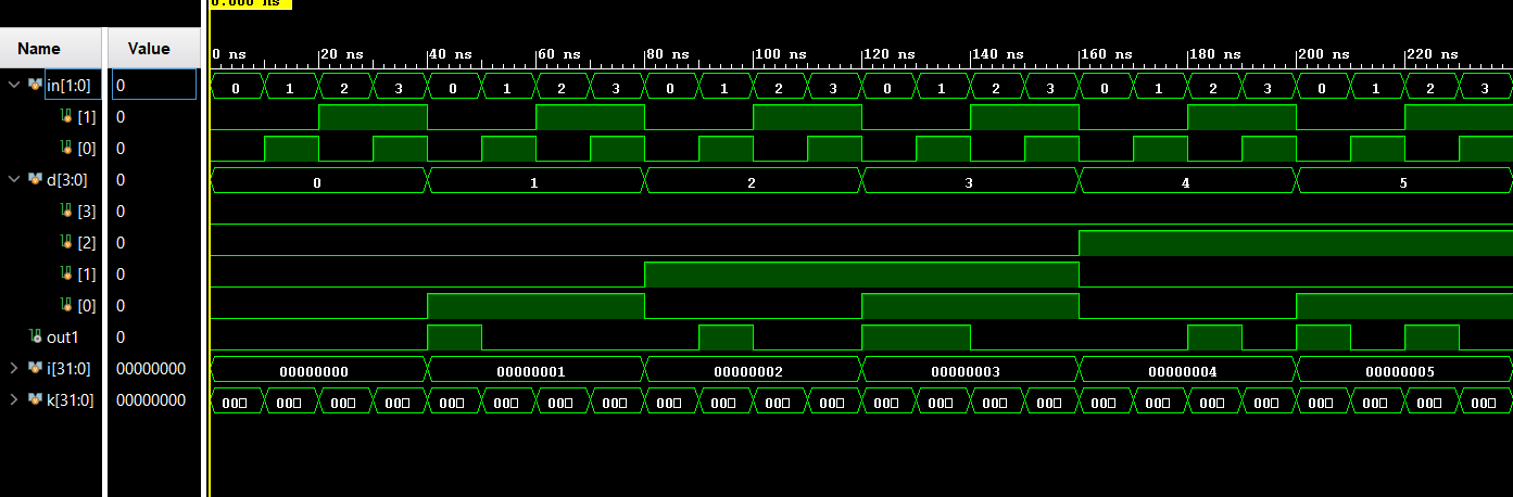
Figure 15:
Simulation of the four to one MUX, showing the results from the
test bench, with the inputs 's', and 'd', and the resulting logic
output 'out1'.
Figure 16:
Vivado code to program the FPGA board with the four to one MUX
logic, using the switches and LEDs as inputs and outputs.
Task
2: Complete the tasks in Section 2. Show your code,
explanation, and demonstrate it in an embedded video. (20
points)
Using Verilog
and Vivado to design a 'Running LED' program on the FPGA board.
Use 4 LEDs on the board, turn on each of them for 1 second
one-by-one. Make sure you have a 'reset' function to reset the
LEDs to the original state.
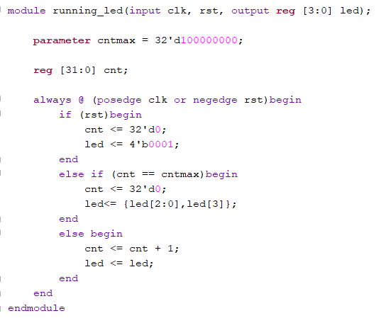
Figure 17:
Vivado code for a Running LED program. With this code we take two
inputs, the clock (clk) and the restart (rst) and output to four
LEDs. Using the clock to change which LED is on every one second,
alternating them down the line and then starting back at the start
when it reaches the end.
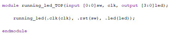
Figure 18:
Vivado code to program the FPGA board with the Running LED
program, using the LEDs to 'run' the light, and a single switch to
restart the running LED.
Task
3: Similar to the example in Section 2, show running
LEDs on all 16 LEDs. Show your code, explanation, and
demonstrate it in an embedded video. (20 points)
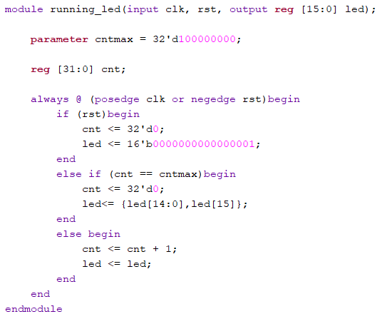
Figure 19:
Vivado code for Running LED using all 16 LEDs.

Figure 20:
Vivado code for programing the FPGA board with the 16 LED Running
LED program.
Task
4: Similar to the example in Section 2, change the
frequency of the 4 running LEDs to half second and demonstrate
it in an embedded video. (20 points)
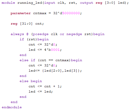
Figure 21:
Vivado code for Running LED at half a second instead of a full
second. This uses the same Vivado as the first one Running LED
program just at half the time.
Task
5: Complete the task in Section 3. Show your code,
explanation, and demonstrate it in an embedded video. (20
points)
Interface the
switches with the 7-segment display on the board.
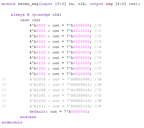
Figure 22:
Vivado code for the seven segment display decoder, taking in a
4-bit input and outputting the 7-bit number that corresponds with
the given input.
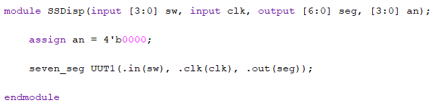
Figure 23:
Vivado code to program the FPGA board to display onto the seven
segment displays on the board. Taking in four switches as inputs
and outputting the binary number from the switches to the seven
segment displays.
WEEK 2 Tasks:
Task 1:
Complete the task in Section 4. Show your code, explanation, and
demonstrate it in an embedded video. (30 points)
Modify the code,
disable any 3 of the 7-segment displays and only show the number
on one of the displays.
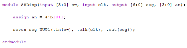
Figure 25: Vivado code to display the input from the switches and outputting them onto one of seven segment displays.
Task 2: Show
"FLC" on three of the display units. Show your code,
explanation, and demonstrate it in an embedded video. (30
points)
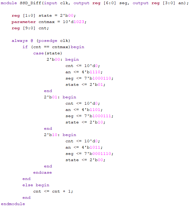
Figure 25: Vivado code to display 'FLC' onto the seven segment displays.
Task3: Roll
"FLC" to the left for every half second. After "F" shifted out
to the left, it should appear on the right hand side. Show your
code, explanation, and demonstrate it in an embedded video. (40
points)

Figure 26:
Vivado code to display 'FLC' onto the display, and having that
'roll' across the displays.