Lab 2 -
Introduction to FPGA
CE 433 Embedded Devices
2024 SpringTasks:
1. Go through all the steps
in this lab instruction, report your code, simulation results,
and the on-board verification results. (30 points)
(on-board verification
results will be in task 3)
Going through this task, we had to code different kinds of gates (AND, OR, XOR) in vivado. you can see the code for the gate below. We then simulate the gates by having an output, 'Y', that was dependent on the inputs, 'a' and 'b', by changing the values of the inputs between 1 and 0 every nanosecond as is shown for each logic gate below, we can see how the output is effected or changes.
Then the later
section of the lab, now that we have coded and simulated the
gates correctly, we then had to take the code of the different
gates and setup the file to program the FPGA, by setting the
inputs to be switches, and the output to a LED. You can see the
setup code for each gate below.
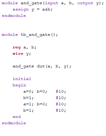 Figure 1: AND gate vivado code,
showing the logic and the test bench code.
Figure 1: AND gate vivado code,
showing the logic and the test bench code.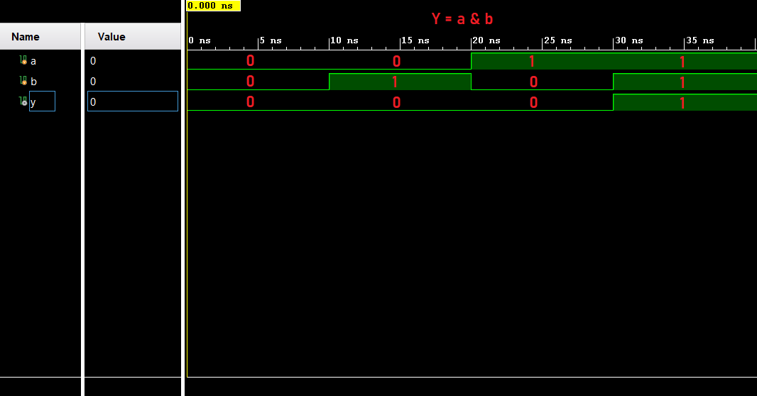 Figure 2: The simulation of the
AND gate, showing how the output 'Y' is affected by the changes
of 'a' and 'b'.
Figure 2: The simulation of the
AND gate, showing how the output 'Y' is affected by the changes
of 'a' and 'b'.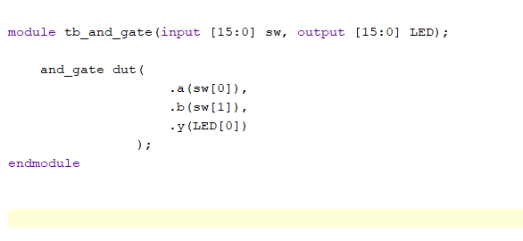 Figure 3: The
FPGA setup code for the XOR gate showing the input switches and
the output LED.
Figure 3: The
FPGA setup code for the XOR gate showing the input switches and
the output LED.
2. Use the same procedure to create XOR and OR gates. Run simulations to verify the logic. (30 points)
This is the same
as task 1, but are implemented for logic gates OR and XOR. The
same simulations to show the relationship between the inputs,
'a' and 'b', and the output, 'Y'. There are also figures showing
the setup code to program the FPGA that can be seen below.
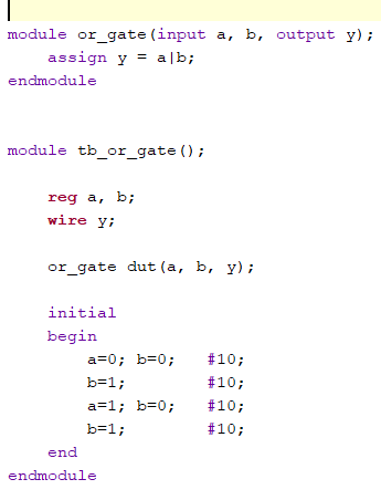 Figure 4: The vivado code for
the OR gate, changing the inputs after 10 NS.
Figure 4: The vivado code for
the OR gate, changing the inputs after 10 NS.
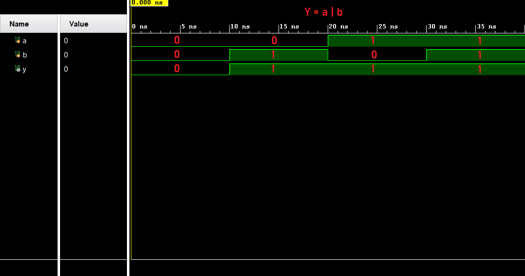
Figure 5: The OR gate simulation, showing the relationship between 'Y' and the inputs 'a' and 'b' using the OR logic.
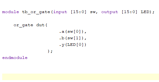 Figure 6: The
FPGA setup code for the OR gate showing the input switches and
the output LED.
Figure 6: The
FPGA setup code for the OR gate showing the input switches and
the output LED.
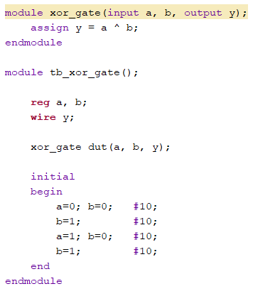 Figure 7: The vivado code
showing the XOR logic changing the inputs every 10 NS.
Figure 7: The vivado code
showing the XOR logic changing the inputs every 10 NS.
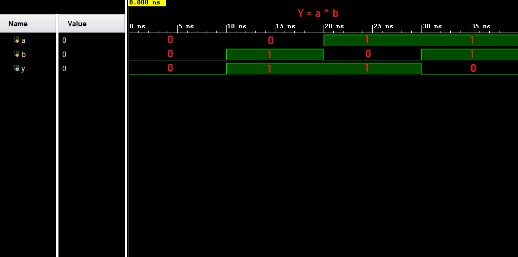 Figure 8: The XOR simulation
showing the relationship between 'Y' and the inputs 'a' and 'b'
using the XOR logic.
Figure 8: The XOR simulation
showing the relationship between 'Y' and the inputs 'a' and 'b'
using the XOR logic.
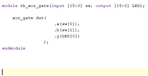 Figure 9: The FPGA setup code
for the XOR gate showing the input switches and the output LED.
Figure 9: The FPGA setup code
for the XOR gate showing the input switches and the output LED.
3. Use both the volatile and nonvolatile methods (QSPI) to program your FPGA. Show videos for the demonstrations. (40 points)
Video 2: Demonstrating a volatile AND gate
Video 4: Demonstrating a volatile OR gate
Video 5: Demonstrating a non-volatile XOR gate