Lab 6
ENGR 338
James Ferguson
Introduction
The goal of this lab is to create both the schematic and layout of NAND, NOR, and XOR gates as well as a full adder in Electric VLSI.
Methods
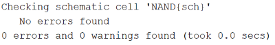
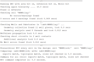
First a NAND gate was designed.
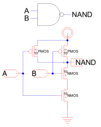
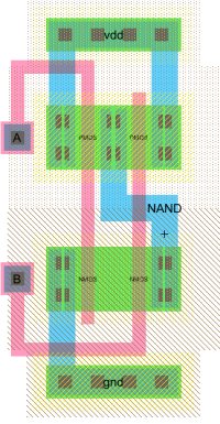
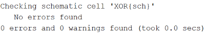
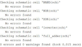
Error checking on both the schematic and layout found no errors.
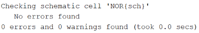
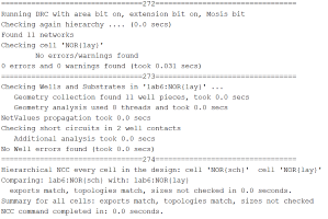
A NOR gate was then designed.
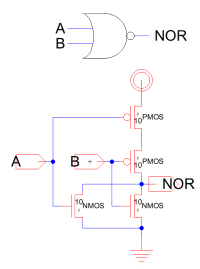
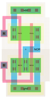
Again, error checking found no problems.
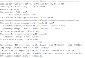
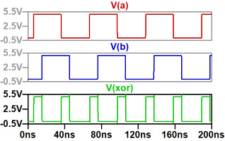
The more complicated XOR gate was then laid out.
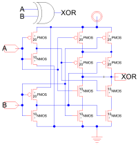
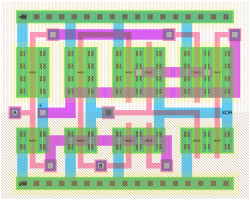
Error checking found no errors.
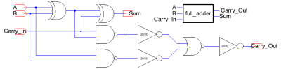
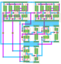
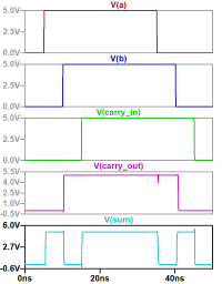
All of the previously designed logic gates where then used to create a full-adder.
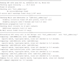
Error checking on the full adder also found no porblems.
Results
Simulations for the XOR gate and the full adder can be viewed below.
Discussion
The designed full-adder performed as expected and is ready to be used to create adders of various widths.