Name: Mason Brady and Ian Van Horn Email: mrbrady1@fortlewis.edu imvanhorn@fortlewis.edu
Course Project
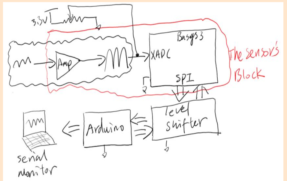
The
purpose of this project is to configure the ADC on the BAYSYS 3 board
to read and convert values from a potentometer. The digitized values
are then to be sent using SPI communication protocal through a level
shifter to an arduino uno. The arduino is programed to recieve the data
and display it.
Figure 1: Refrence diagram
Part 1: Configure the ACD
The adc configuration code was taken from an online tutorial :
https://digilent.com/reference/programmable-logic/basys-3/demos/xadc
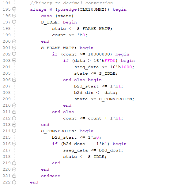
Figure 2: ADC code sample
The ACD is largley gnerated through an IP form the wizard. The above
code is a binary to decmil conversion to display on a seven segment
display. The output is also displayed on the Baysys LEDs. All code
regarding the ADC is taken from the online tutorial.
The wire connections are also taken from the tutorial.
Part 2: Output data in SPI
format
The BAYSYS 3 is configure as a leader transmitter. For
this project, every other group cofigured the board as a follower
transmitter. The idea behind the different configuration is that the
resources are available in the textbook to properly configure the
BAYSYS, byt we had no information on SPI with an arduino. By having the
BAYSYS be the leader it seemed easier on the backend arduino recieving.
Figure 3 shows the code used to impliment the leader transmitter in the
ADC testbench.
Figure 3: Code implimentation for leader follower
The arduino clock in the SPI library is 2MHZ. For some reason the
BAYSYS clock wizard only goes to 4MHZ so a custom divider was used to
lower the frequency in case the SPI library was used on the backend.
The data from the ADC is 16 bits. The sensitivity of the signal is so
high only 8 bits is needed, even that is very sensitive. Data is
wirtten out at the eigith cycle of the positive edge of the sck signal.
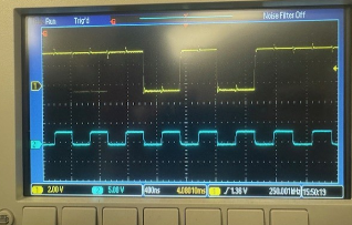
Figure 4: Example output of the SPI/ADC code
In figure 4 the blue plot is SCK and the yellow is the MOSI line.
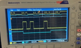
Figure 5: Output of the SPI/ADC with CS
Now the blue line is the chip select line signaling when data is being
sent.
Part 3: Recieve data with
arduino
The output from the BASYS 3 is suprisingly clean. The next step is to
recieve data with the arduino. The SPI library did not work, we are not
sure why. Usually an arduino is configured as a leader, there are not
too many resources on configureing one as a folower. However, because
most of the complexity is done on the BASYS it is possable to write a C
script to recieve the data. This has complexities. The communication is
so fast that polling for edges of sck and cs in void loop will not
reliably read data. To aboid this problem, an interrupt servise routine
was configured to detect rising edges of sck.
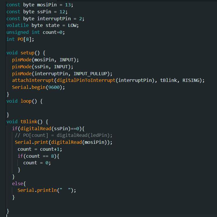
Figure 6: C code
Every rising edge of sck the service rutine is entered. If ss (cs) is
low, signifing data is being transported, then the stat of mosi is
serial printed. Because of the precise sck timing exactly 8 bits are
printed before ss is low again. The main issue with this approach is
that the serial print is very very slow. So slow that by the time the
ISR is finished, several other sck cycles have passed at a normal
frequency for SPI. To avoid this, the sck frequency was slowed to 1khz.
To solve this issue more efficently, the vlaues of data should be
pushed into an array. Once filled, the ISR should be disabled and the
array should be printed, then the ISR should be enabled again. Whole
packages of data would then be missed but because the transmission rate
is so fast this would not matter. This fix was not iplimented due to
time and the high level of work already required to get to this stage.
Part 4: Results
The module works as expected. Data values arre accuratly and
continously read by the arduino. However, the ADC is very very unstable
in reaing the potentometer. This could be because of a low quality of
breadboard or potentometer. There could be a small error in the adc
code or transmission but this seems unlikley as data is perfectly
transmitted during steady state. For this reason, two demos are shown,
one at steady state and one with a potentometer input.
Video 1: Steady state demo
Video 2: ADC input demo
Conclusion: This project was equally by Ian Van Horn and Mason Brady
We both invested many hours in this project. Many issues were
uncovered. The first used level shifter created massive noise and was
unsueable. Writing the testbench for the SPI leader transmitter was
difficult. To throubeshoot the SPI module seemed impossable so we ended
up writing a simple reciever from scratch which had a lot of nuace.
Overall, the project required a lot of problem solving and learning and
would not have been possable without large scale collaberation.