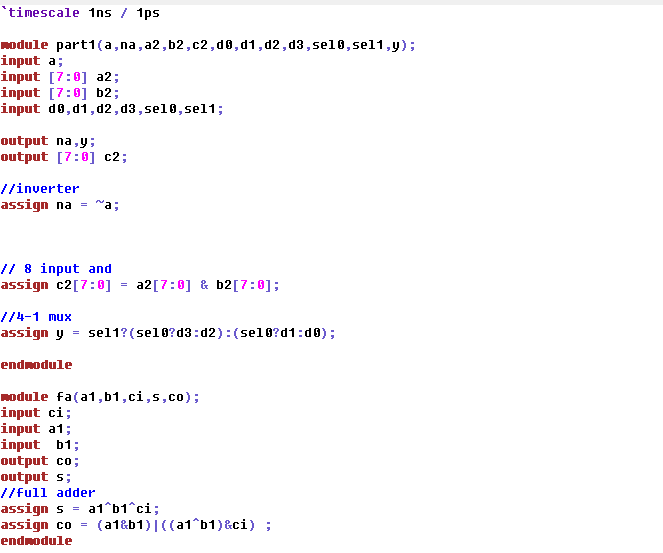
Figure 1-1: Logical definitions for all blocks
All gates were made in the same module. The 2 bit full adder is
implimented later as 2, 1 bit full adders. The 4-1 MUX is defined using
nested conditional statments.
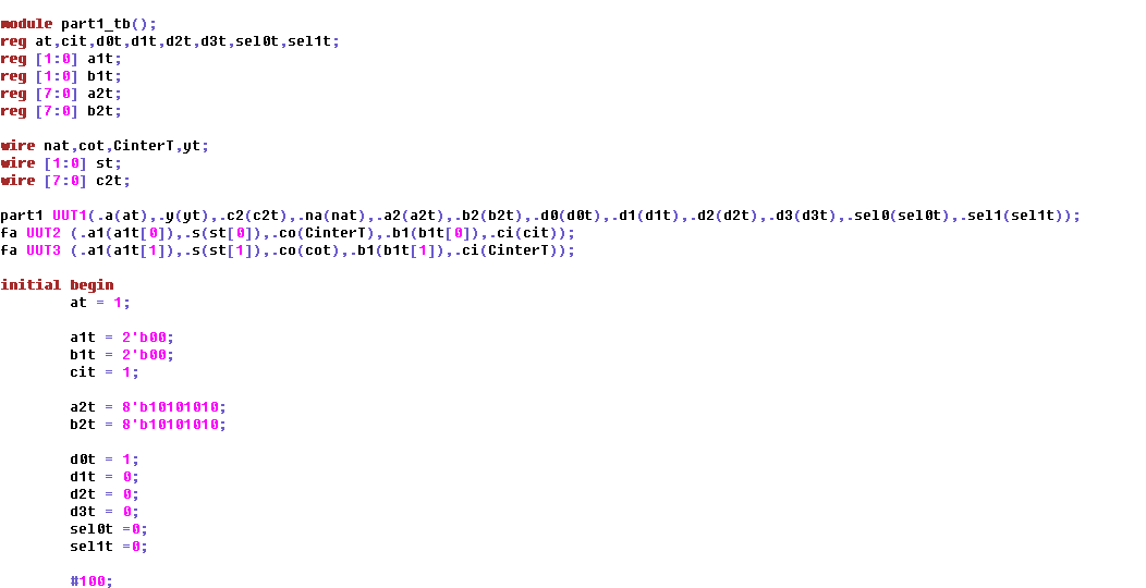
Figure 1-2: Simulation testbench for all logical blocks
3 cycles of switching inputs are not shown due to redundency. The full
adder is nested so that carry out from the first is carry in to the
second.
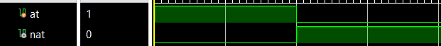
Figure 1-3: Inverter simulation results where at is input nat is output.
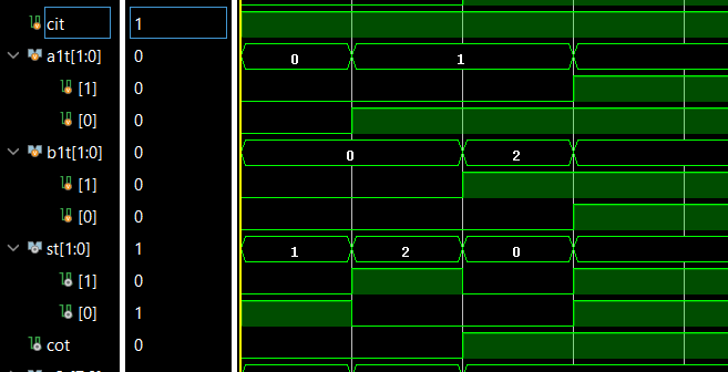
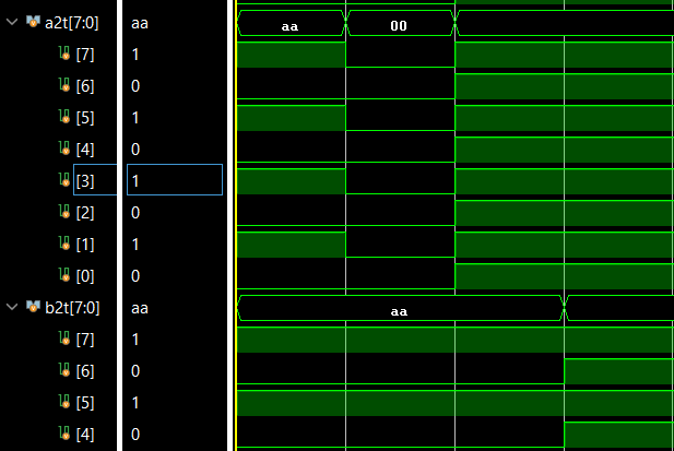
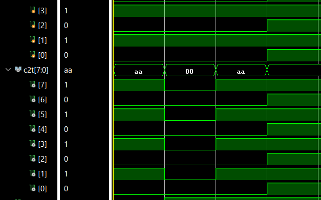
Figure 1-3: 2 bit full adder simulation, intermediate carry not shown
Figure 1-4: 8 input and simulation
c2t is the result of anding the respctive bits in b2t and a2t.
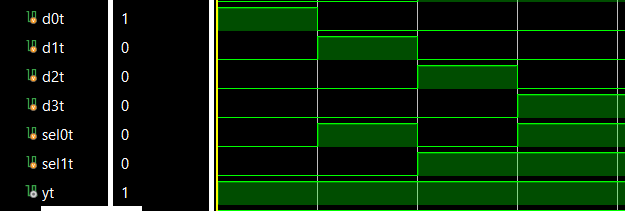
Figure 1-5: 4-1 MUX simulation
The output (yt) is always high. This is because as the input (d0t-d3t)
is cycled the binary selection (sel0t,sel1t) is stepped up by 1.
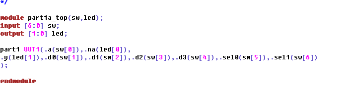
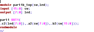
Figure 1-6: Inverter and 4-1 MUX FPGA implementation code
The inverter was assigned to the first switch and LED. The MUX uses the
second led and next 6 switches.
Video 1-1: Demonstration of inverter and 4-1 MUX
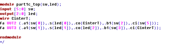
Figure 1-7: 2 bit full adder implimantaion code
The 4 rightmost switches are 2, 2 bit binary inputs. The 5th rightmost
is carry in. The added numbers are displayed on the leds
Video 1-2 Demonstration of 2 bit full adder
Figure 1-7: Implimentation code for 8 bit and gate
Video 1-3: Demonstration of 8 bit and gate
Due to the quality of the switches on the board, an input is
ocassionally misred resulting in an LED being lit that should not be.
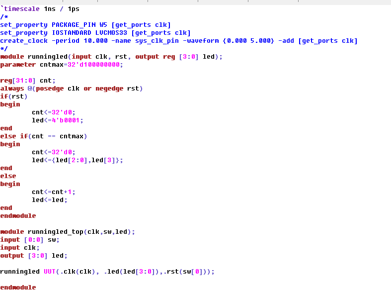
Task 2: Running led (20 points).
Figure 2-1: Code to make 4 leds cycle every second
The clock portion of the constraints file was uncommented. cntmax is
set to one hundred million as the 100MHZ ocillator is used for timing
and the LED should cycle every second. If the reset switch is
activated, the first led is on only. Otherwise, count is incrimented
until cntmax is reached and the LED is cycled.
Video 2-1: Running Led demonstration
Task 3: Running led, 16 LEDs (20 points).
Figure 3-1: Modified code from Figure 2-1 for 16 running LEDs
The size of "led" was changed to 15. This was also changed in the
testbench.
Video 3-1: 16 running LEDs
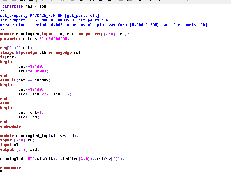
Task 3: Running led, 4 LEDs, .5
sec (20 points).
Figure 4-1: Modified code from Figure 2.1 for LEDS to update every .5
sec
cntmax was changed to half of its value.
Video 4-1: .5 sec running LED demonstration
Task 4: SSD (20 points)
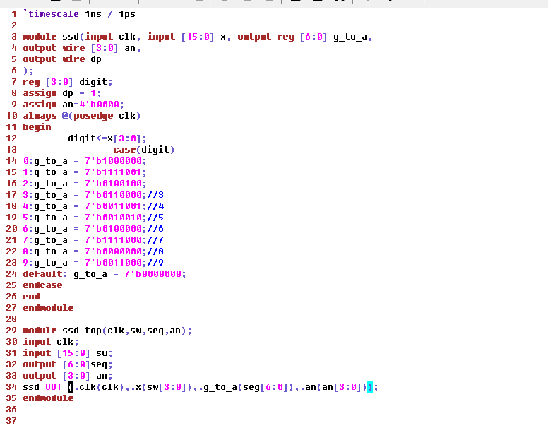
Figure 4-1: Code to change SSD from binary switch input
an is set to 4 zerozs to enable all 4 ssd panels. Digit is the input of
the first 4 switches. As a binary number is entered with thes switches,
whenever clk is updated, the corrosponding number is displayed on the
ssd. The binary codes for the ssd were determined as the binary number
is sections g-a on the posted ssd diagram.
Video 4-1: SSD counting demonstration
Week 2
Task 1: Section 4 (30 points)
Figure 1.1:Modification to only light one segment of the SSD
The variable an defines which of the 4 SSD segments are on. To turn 3
off set 3 of them to 1 to disable the pnp bjt transistor connected to
them.
Video 1.1: Demonstration with 3 SSD segments off
Task 2: Display FLC (30 points)
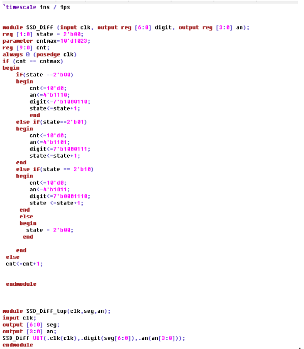
Figure 2.1: Code to display FLC
The portion of the SSD that is lit is kept track of by an which is
diffrent for each if statment. The varable "state" is incrimented which
cycles which "an" and which digit is shown on the board. This is cone
so fast it appears all are on the board simultaniously.
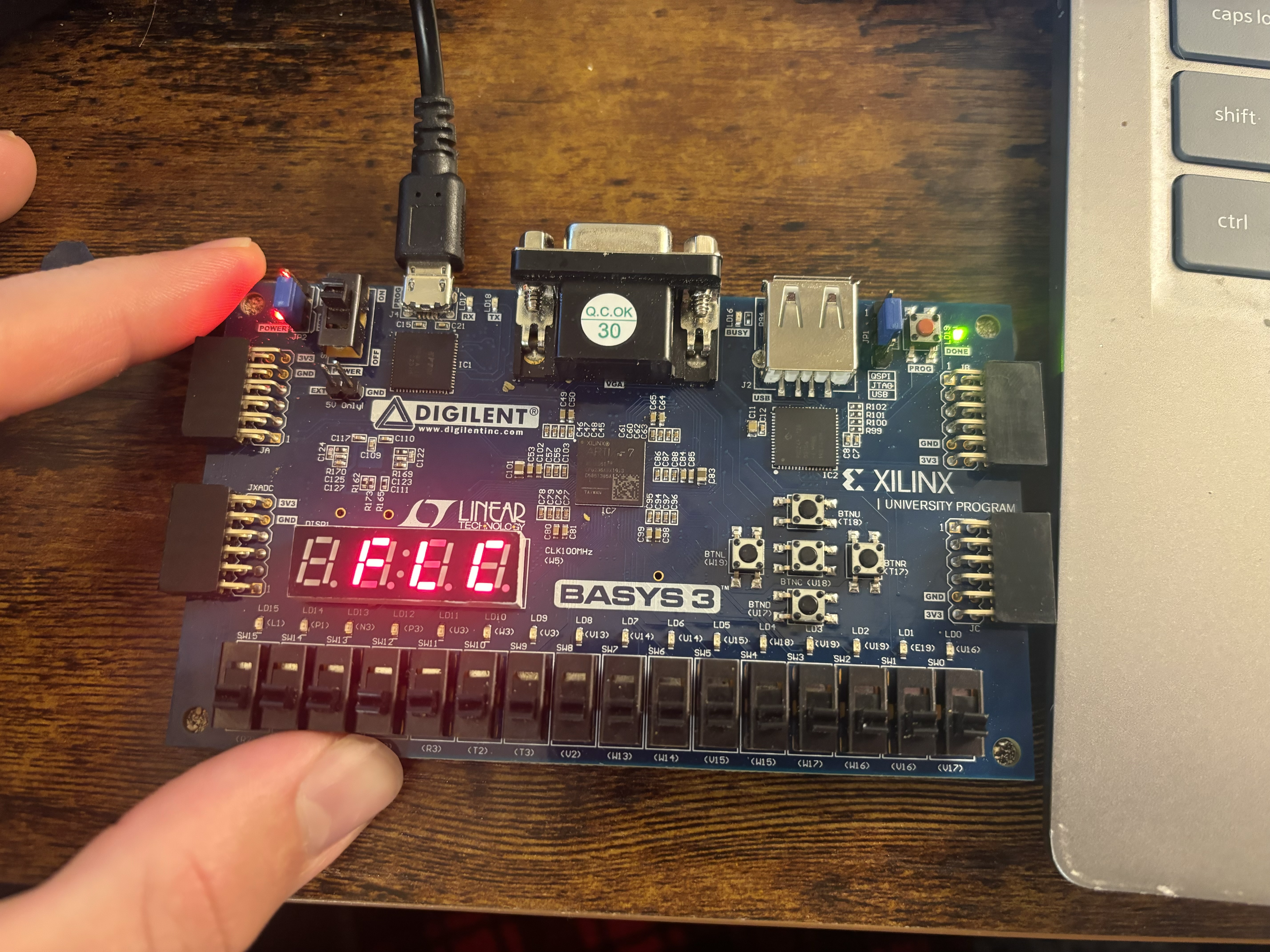
Figure 2.1: Display of FLC on FPGA
FLC is shown as an image not a video because nothing on the board is
changing over time.
Task 3: Roll FLC (30 points)
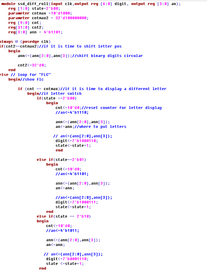
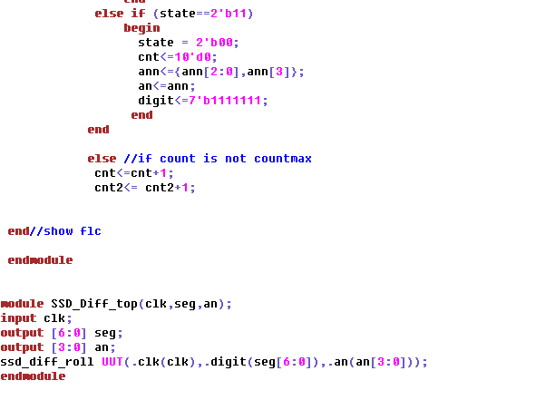
Figure 3.1: Code to display and roll FLC
This code is similar to that of Figure 2.1 except with an extra loop to
update the varable ann. Ann is shifted left and defined which 3 SSD
segments are lit. An is then assigned to be ann when a state is
selected to display a digit. This is because an is a defined varable
that cannot be shifted. A fourth state is needed to shift ann a fourth
time in the state loop it writes each letter to the same segment every
iteration. Then it is shifted 1 extra time every second in the outer
loop to roll the letters.
Video 3.1: Scrolling FLC demonstration
Conclusion: This lab sucessfully taught more complex combinational
logic as well as introducing the SSD and clocked logic