Name: Ian Van Horn Email: imvanhorn1@gmail.com
Lab 2 FPGA Basics
This lab
introduces the basics of Vivado and FPGAs
This lab requires Vivado and the BASYS 3 FPGA
Task 1: Repeat Lab Instructions.(30 points).
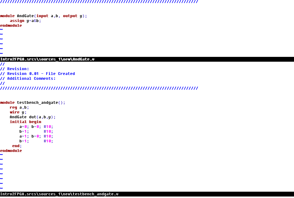
Figure 1.1: Gvim code for an and gate simulation
y is assigned as the result of anding input A and B. In the testbench a
and b are toggled so a simulation shows all results of the and logic.
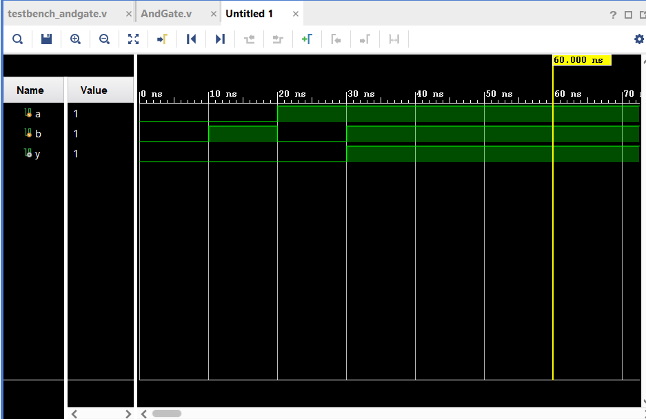
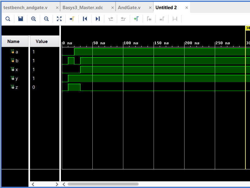
Figure 1.2: Simulation results from code in Figure1.1.
The results of the simulation confirm that y is always the result of a&b.
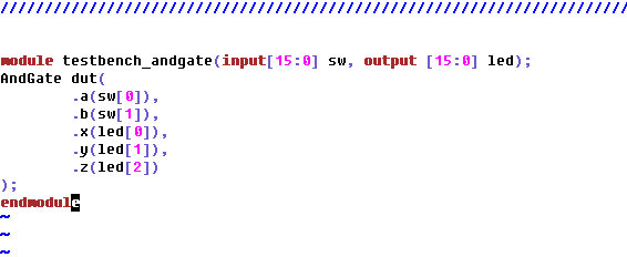
Figure 1.3: Gvim code for testbench on FPGA
The inputs are assigned to the rightmost and second rightmost switches
on the FPGA. The result of anding the states of the switches is
displayed on the rightmost LED.
Video 1.1: Demonstration of and gate on FPGA.
In video 1.1, LD0 shows the state of the and gate and V17 and V16 are
the inputs. The FPGA in programed with the non-volital tequnique
(Pressing the PROG button did not change the program showing the
program is loaded to on board memory)
Task 2: Simulate or and xor(30 points).
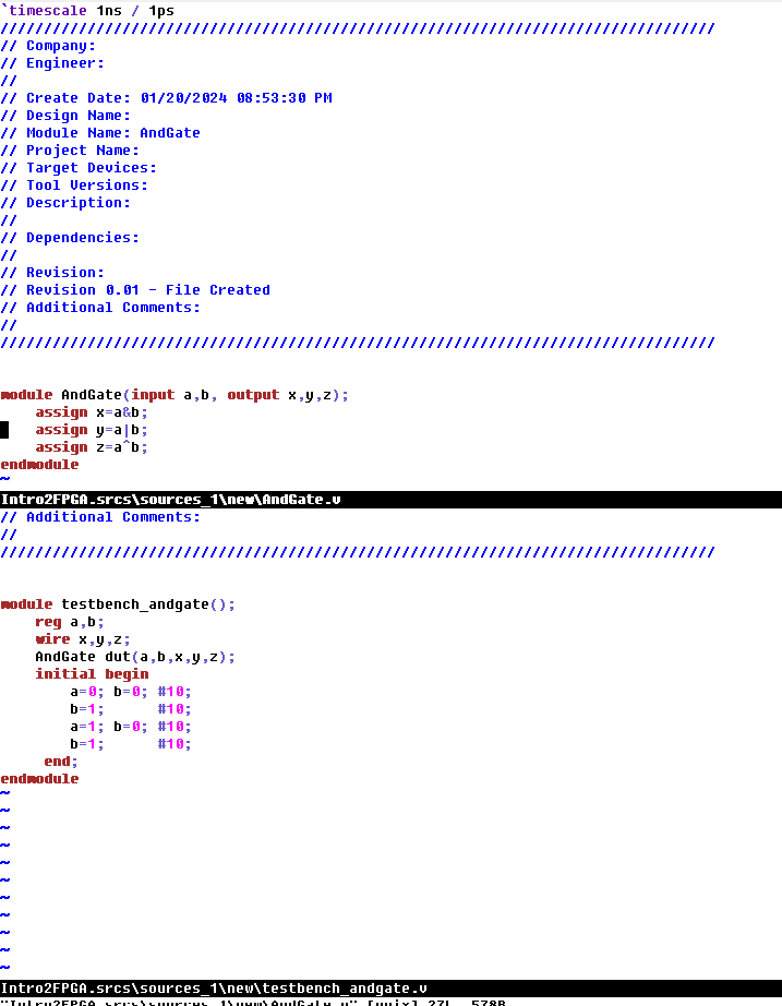
Figure 2.1: Gvim code to simulate and, or, and xor logic
Now x shows and logic of a and b, y shows or logic, and z shows xor logic. Again a and b are toggled to show all combinations.
Figure 2.2: Simulation of code in Figure 2.1
The simulation confirms the logic is being done properly
Figure 2.3: Gvim code for and, or, xor testbench on FPGA
Now or logic is shown on the second to rightmost led and xor on the 3rd to rightmost. The inputs are the same as the and gate
Task 3: Program with volatile
and non-volatile, demonstrate with videos(40 points).
Video 3.1: Volatile example
In video 3.1 the board is first unprogrammed. The board is then
programmed and the logic is shown. LD0 shows and logic, LD1 shows or
logic, LD2 shows xor logic. V17 and V16 are inputs. The board is then
powered down, then back up. The program is lost.
Video 3.2: Non-Volitile example
In video 3.2, the jumper position is changed to the QSPI position from
the JTAG position and the program button is pressed. This loades the
program to the boards memory. The logic is demonstrated (same as Video
3.1). The board is powered down then back up and the program is saved.l
Conclusion: This lab instructed on how to uplode HDL code to an FPGA using Vivado