Name: Ian Van Horn Email: imvanhorn1@gmail.com
Midterm
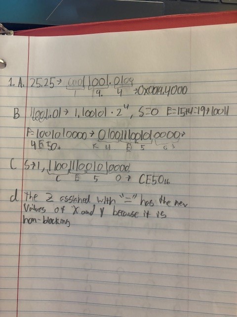
Task 1: Fundimentals(20 points).
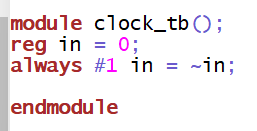
Task 2: Simulate 2ns clock
waveform(10 points).
Figure 2-1: Code for clock waveform
No module besides a testbench is needed
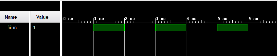
Figure 2-2: Sinulation for 2ns clock waveform
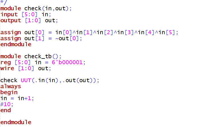
Task 3: Even/odd number of ones
checker(10 points).
Figure 3-1: Code for checking even/odd number of ones
The xor statment will produce a 1 if there are odd number of ones and a
0 when there is an even number of ones. For this spicific case this is
always the LSB of the result and the MSB is the compliment of the LSB.
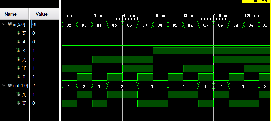
Figure 3-2: Simulation results
Task 4: State Machienes(60 points).
Part A:
Part B:
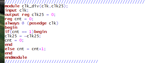
Figure 3-2: Clock Divider module
This module produces a 25MHZ clock from the 100MHZ clock for the VGA
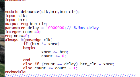
Figure 3-3: Debounce module
The psudo clock from the switch for the decoder needs to be debounced.
The delay is set to 1s because of the poor switch quality.
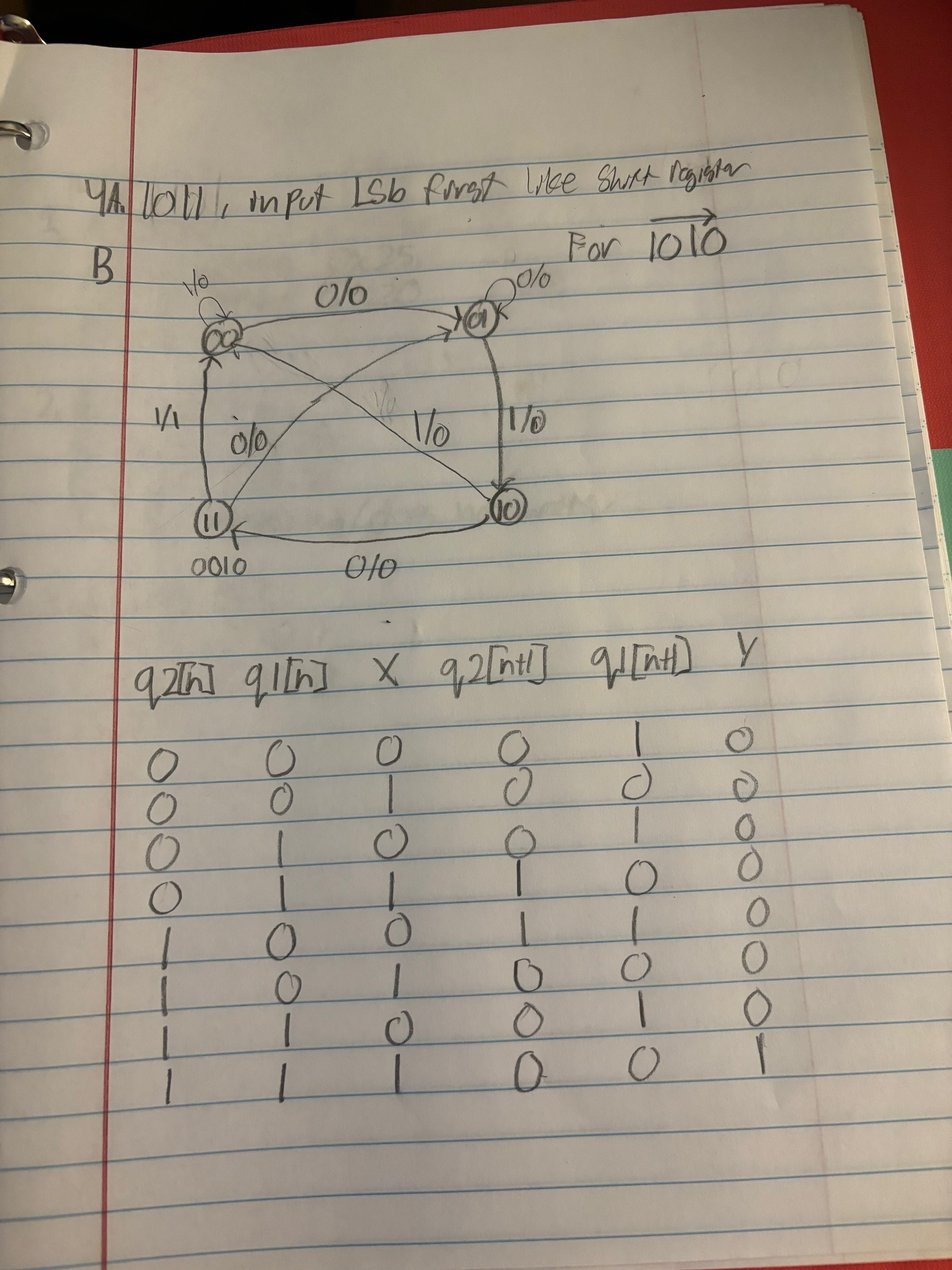
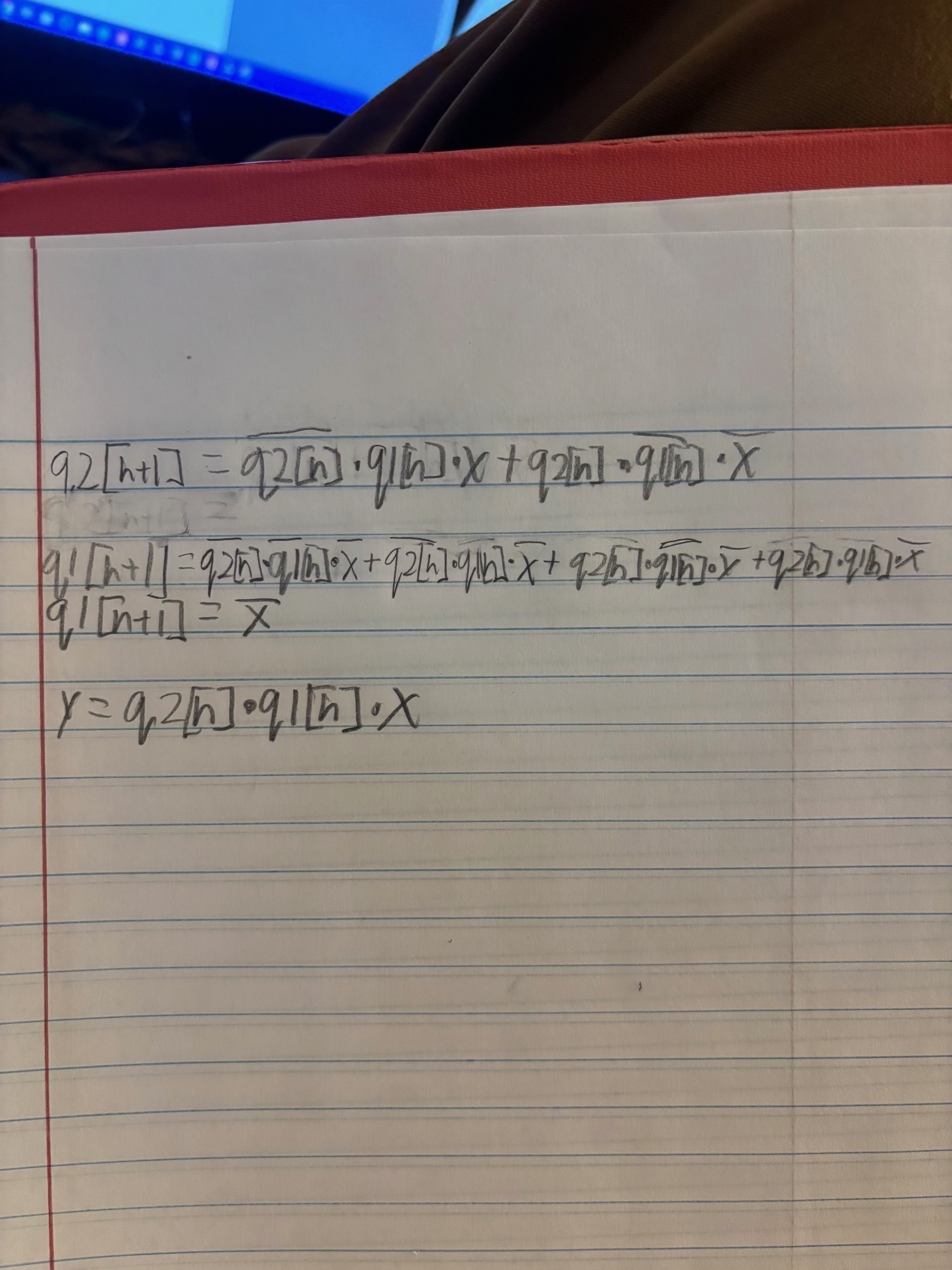
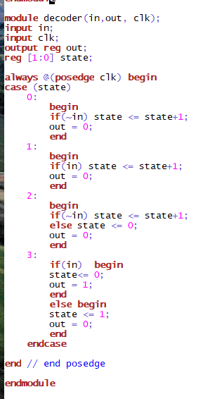
Figure 3-4: Decoder module
This module detects an input of 1010 from the users searial input
(assuming the LSB is the first input like in the SIPO shift regester).
Behavioral modeling is used rather than the derived expressions.
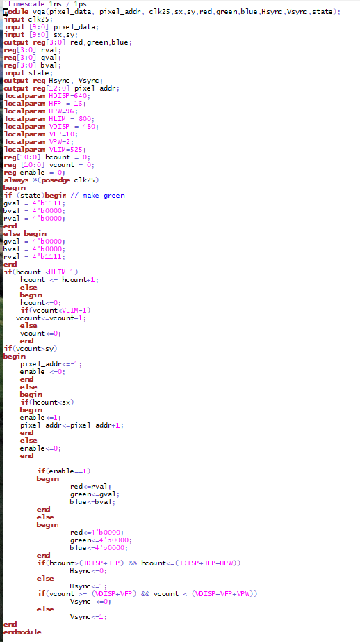
Figure 3-5: VGA code
Now the vga has an extra input from the decoder which chooses which
color to diaplay
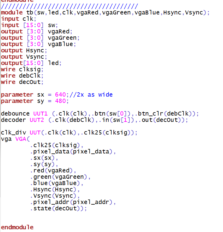
Figure 3-6: Testbench linking all modules
The testbench properly connects all modules