ENGR 433 - HW 4 2024 Spring
Name: Ian Van Horn
Email: imvanhorn1@gmail.com
HW 4
This assignment introduces memory
This lab requires vivado
Task 1: Section 1-3 Simulations. (20 points).
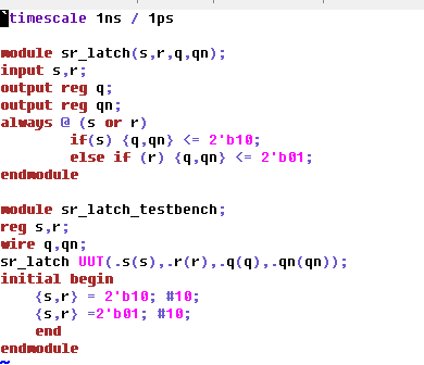
Figure 1-1: SR latch code and testbench in Gvim
SR latches have a set and reset functionality and a memory state. When
set is 1 q is 1 and qn is 0. When reset is 1 q is 0 and qn is 1. When r
and s are both 0, an q is the previous value of q and qn is the
previous value of qn. The set and reset logic is done with an if/else
if statment in this code.
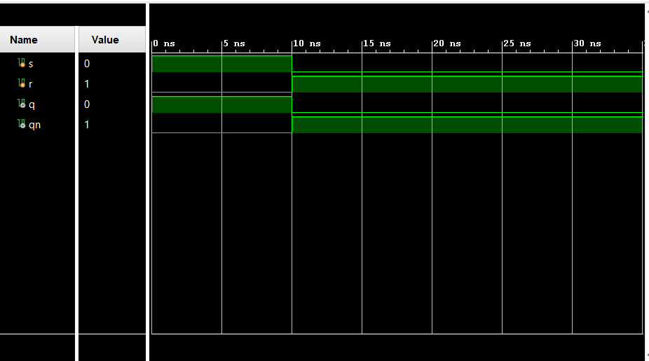
Figure 1-2: SR latch simulation
This simulation does not show a memory state as it was generated the same way as the simulation on the website.
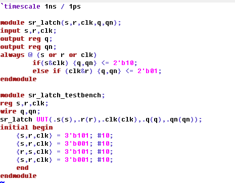
Figure 1-3: SR flip flop code in Gvim
This is a clocked SR latch. Set and reset are only read by the latch
when the level of the clock is 1. Otherwise, the latch is in a memory
state. This is because each input is anded with the clock then passed
to S and R. When clock is 0, the and gates produce a 0 which is a
memory state. When the clock is 1, the and gated produce whatever S and
R are.
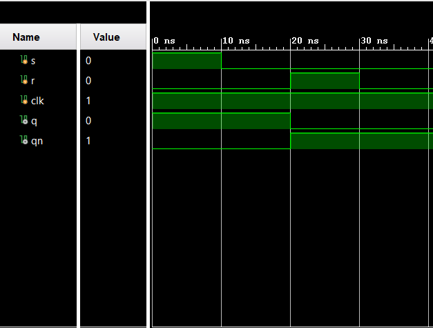
Figure 1-4: SR flip flop simulation
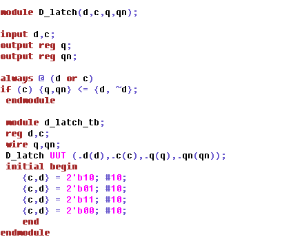
Figure 1-5: D Latch code in Gvim
This is similar to the SR ff, but there is only 1 input (data). The
data is passed to q when the clock is 1. Otherwise, the sr latch is in
a meory state. The input is passed to an and gate and anded with the
clock and another gate takes the compliment of the and gate and the
clock. Form there the logic is the same as the SR flip flop
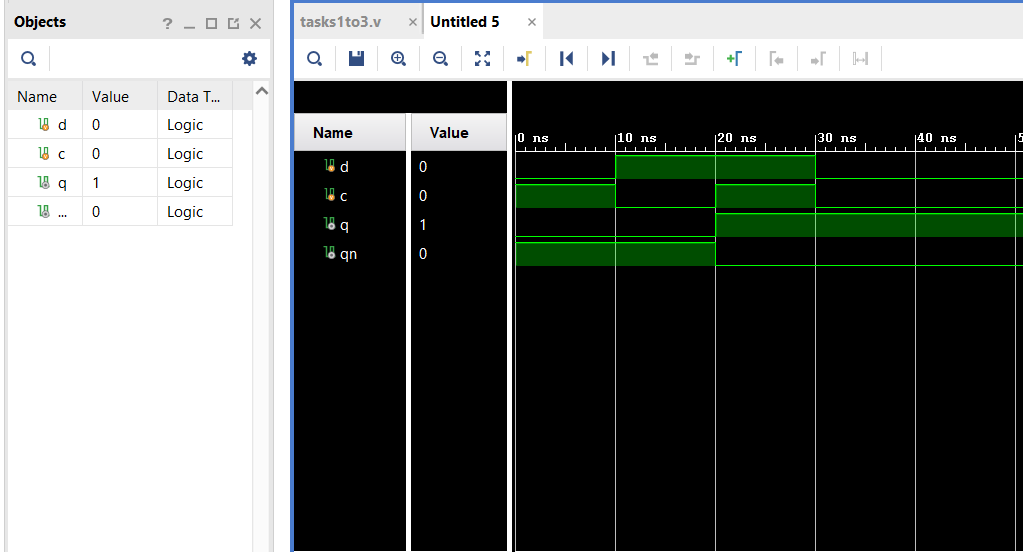
Figure 1-6: D Latch simulation results
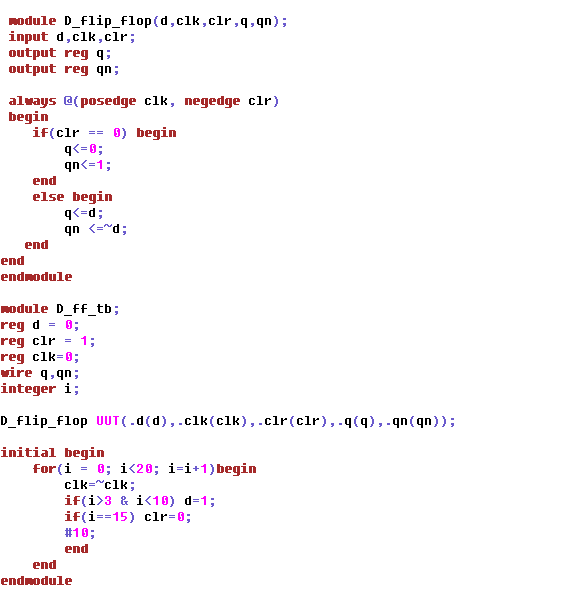
Figure 1-7: D flip flop- edge triggered code in Gvim
Where a D latch passes input data to Q when clk is 1, an edge triggered
DFF passes it when the clock has an edge, in this case a rising edge.
This DFF also has a clear function. When clr has a falling edge q is
reset.
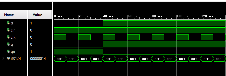
Figure 1-8: Edge triggered DFF simulation
Task 2: Debounce circut with Schmitt trigger (20 points).
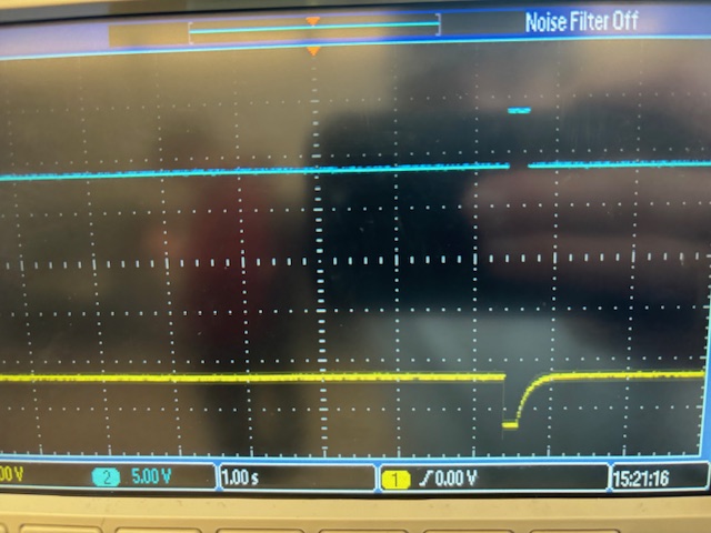
Figure 2-1: Button press signal before and after debounce circut, probed at node 1 on the circut diagram (Before capacator)
The input from the button is shown on the yellow ocilliscope line. The
output in the blue. The Schmitt trigger provides a sharp edge on the
output.
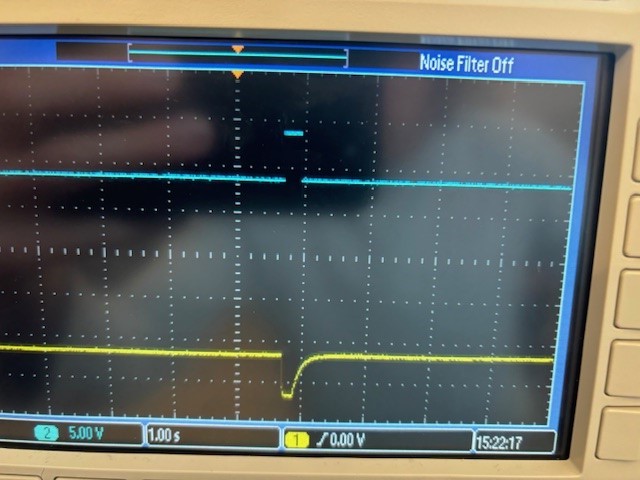
Figure 2-2: Circut probed at node 2, after RC filter
Before the schmitt trigger, the signal is filtered. The yellow signal
is the filtered button input. The sharp noise and corners found in
Figure 2.1 are gone.
Task 3: Section 4&5 Simulations. (20 points).
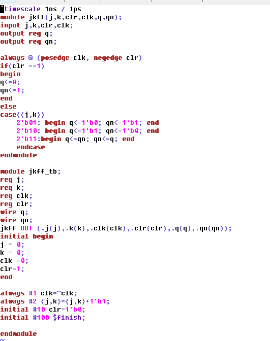
Figure 3-1: Edge triggered JKFF code in Gvim
This circut emulates an sr latch but eliminates the unused state. This
is accomplished by using a DFF as well as or and and logic.
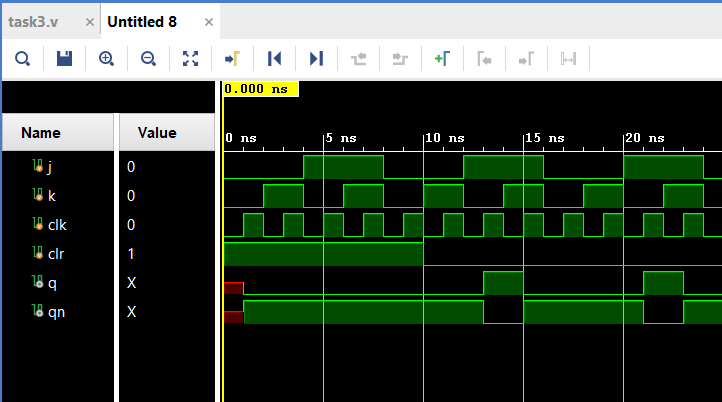
Figure 3-2: JKFF simulation
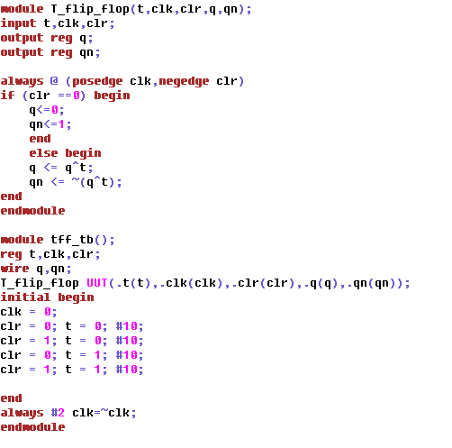
Figure 3-2: TFF code in Gvim
A TFF is created by shorting both inputs of the JKFF to logic 1. When
the input is at logic 1 the output of the TFF toggels, when at 0 it
does not change
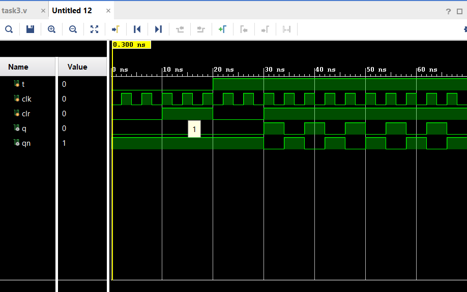
Figure 3-2: TFF simulation
Task 4: Work from section 8 (ROM) (40 points).
Memory is constructed from registers which are constructed from flip
flops. To find the data there is a address bus. To read and write data
there is a data bus.
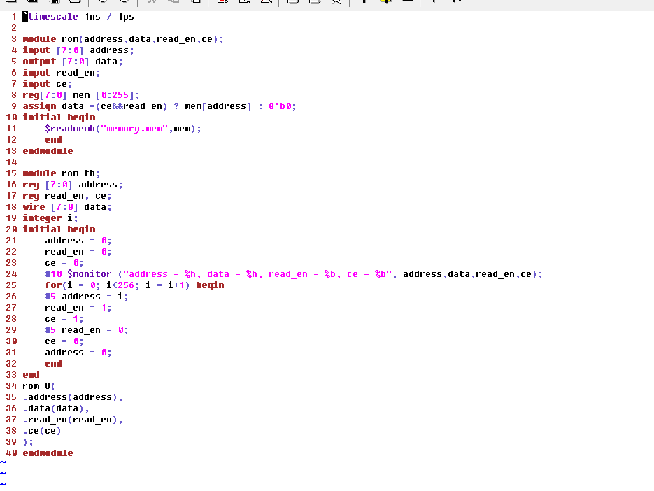
Figure 4-1: ROM module and testbench for reading 8 bit binary numbers
The address provides the location of a stored value, it needs to be
scaled with the depth of the memory. Data holds the calue read form the
memory file. $readmem is subscripted with a H or a B to to indicate hex
or binary.
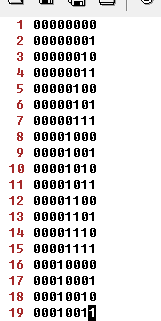
Figure 4-2: Memory file to be read
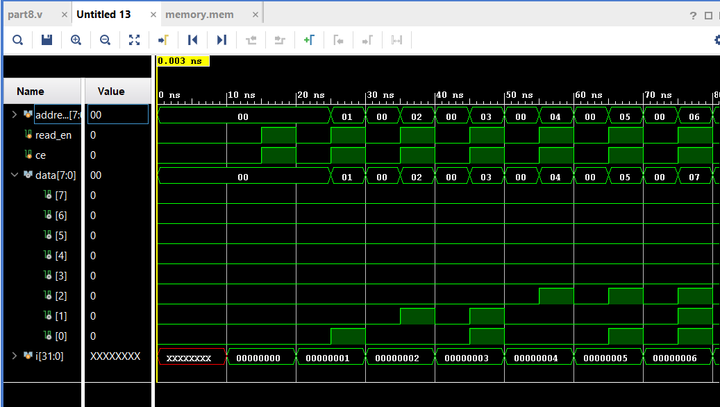
Figure 4-2: Binary ROM simulation
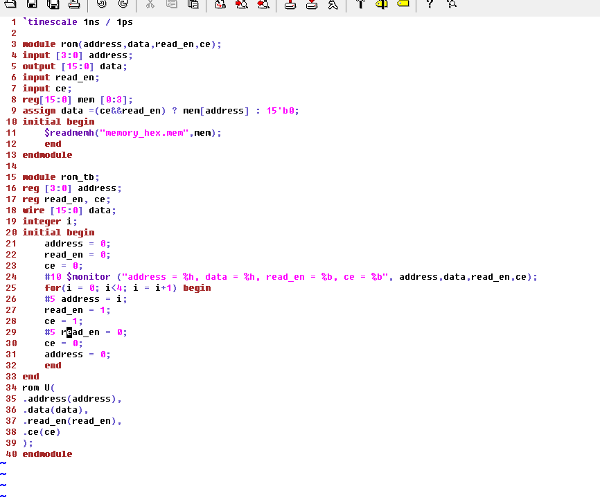
Figure 4-4: ROM code modified for 4 digit hex numbers
The length of "data" is doubled as 4 hed digits are 16 bits
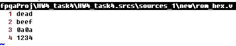
Figure 4-5: 4 digit hex digits in memory file
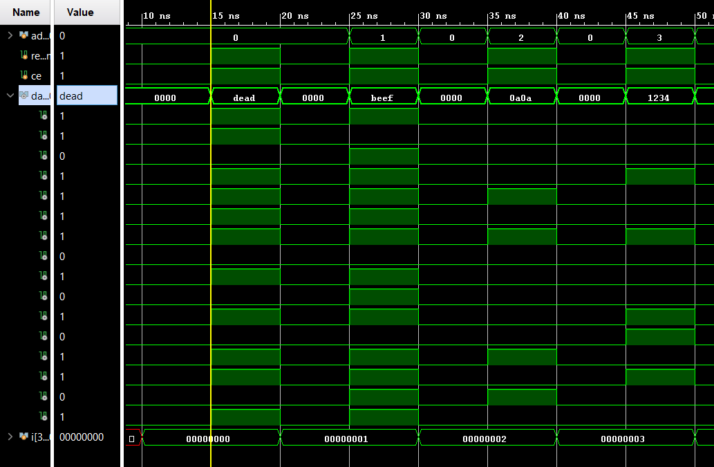
Figure 4-6: Simulation results for hex ROM
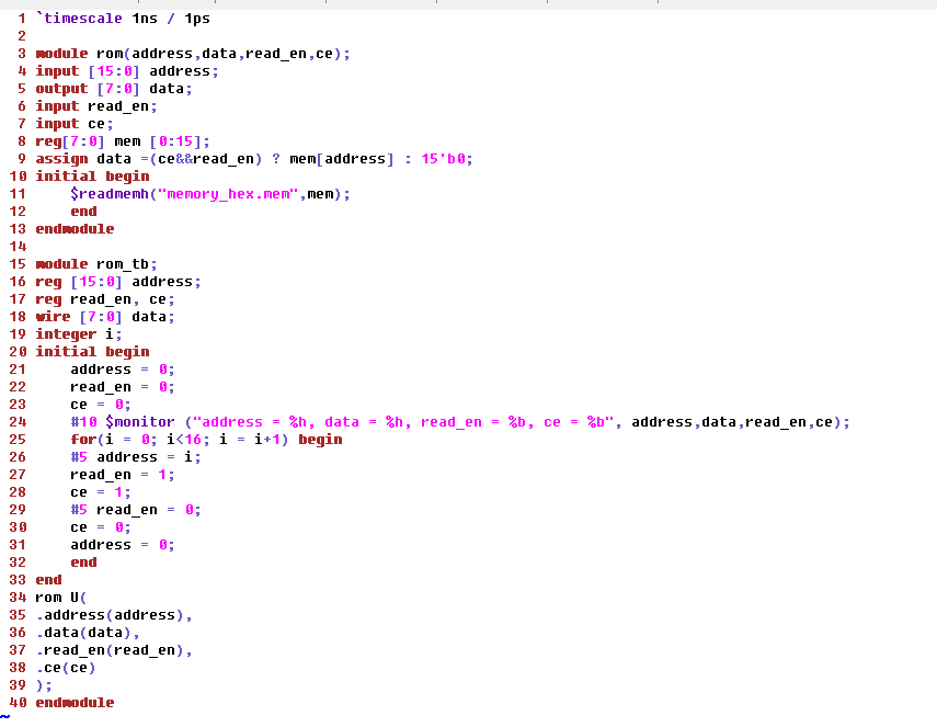
Figure 4-7: ROM code for 8 bit hex (2 digit)
Now the address is 8 bits becaus ethe data is 8 hex numbers.
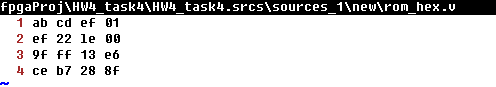
Figure 4-8: Memory file with 8 bit hex numbers
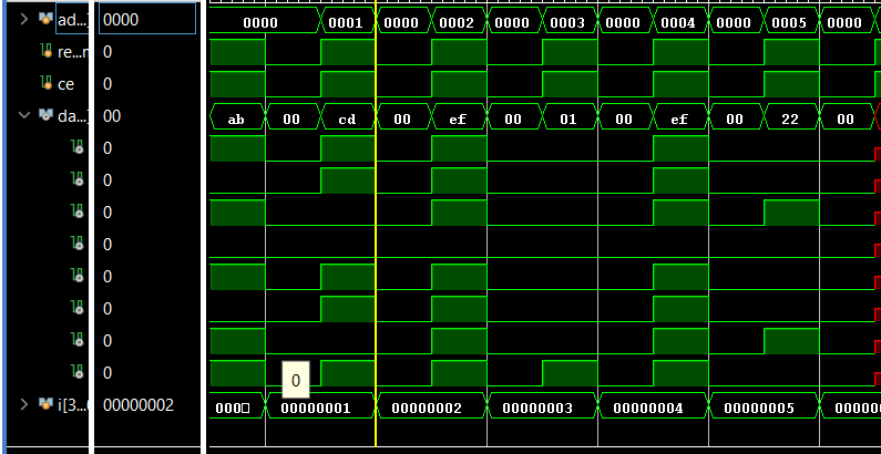
Figure 4-9: 8 bit hex ROM simulation
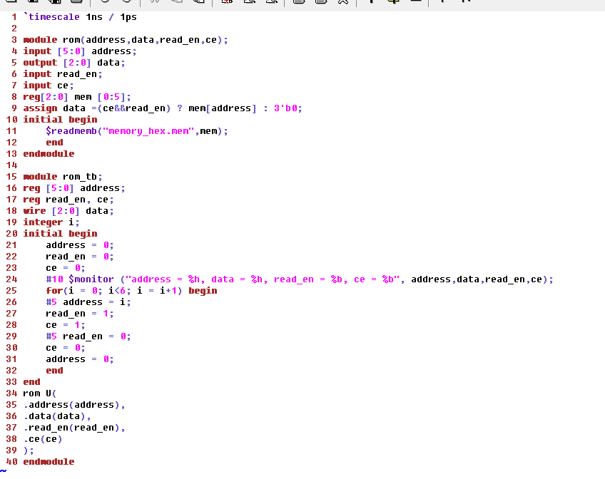
Figure 4-10: ROM code for 3 bit binary numbers
Data is changed to 3 bits for 3 binary numbers

Figure 2-11: Memory file with 3 bit binary numbers
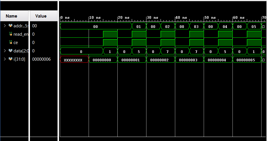
Figure 4-12: ROM simulation with 3 bit binary numbers
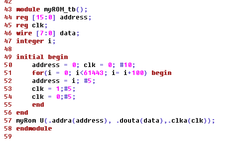
Figure 4-13: Testbench for IP block
The rising edge of clk sends an address, hence data is extraceted on a rising clock edge
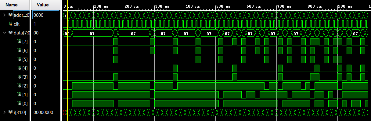
Figure 4-14: IP block simulation
Conclusion: This homework introduced logical memory blocks and ROM