Name: Ian Van Horn Email: imvanhorn1@gmail.com
HW 3 SSD
This lab
introduces the SSD and more advanced HDL programs
This lab requires Vivado
Task 1: Half and Full adders(10 points).
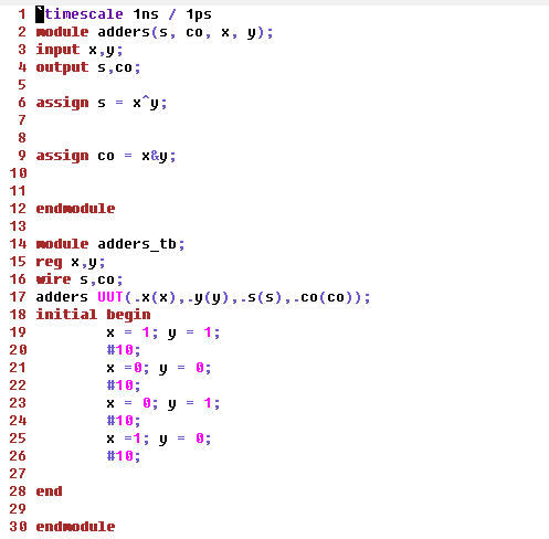
Figure 1-1: Half adder code in Gvim
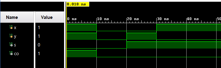
When either input bits are high, the sum is high as the LSB is 1. When
both or neither or high the LSB is 0 so the sum is 0. When both are
high carry out is 1 as the MSB is 1.
Figure 1-2: Half adder simulation
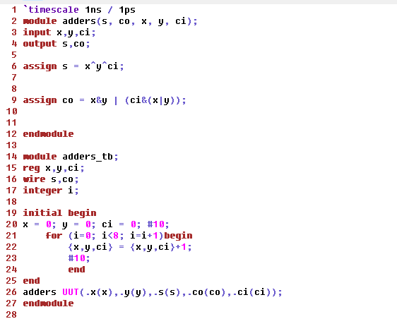
Figure 1-3: Full adder code in Gvim
This is similar to the half adder but with a extra bit for carry in.
This means that in addition to the half adder logic when all 3 bits are
high than sum and carry out are both 1 ad the LSB and MSB are both 1
after addition.
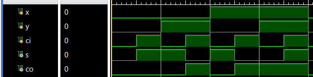
Figure 1-4: Full adder simulation
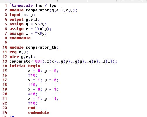
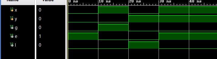
Task 2: Comparator(10 points).
Figure 2-1: Comparator code in Gvim
Comparators compare the input values. For this comparator if x is
greater than y g is 1. IF x and y are the same e is 1. If x is less
than y l is one. All non-high outputs are 0.
Figure 2-2: Comparator simulation results
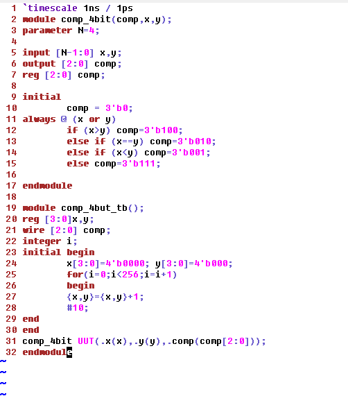
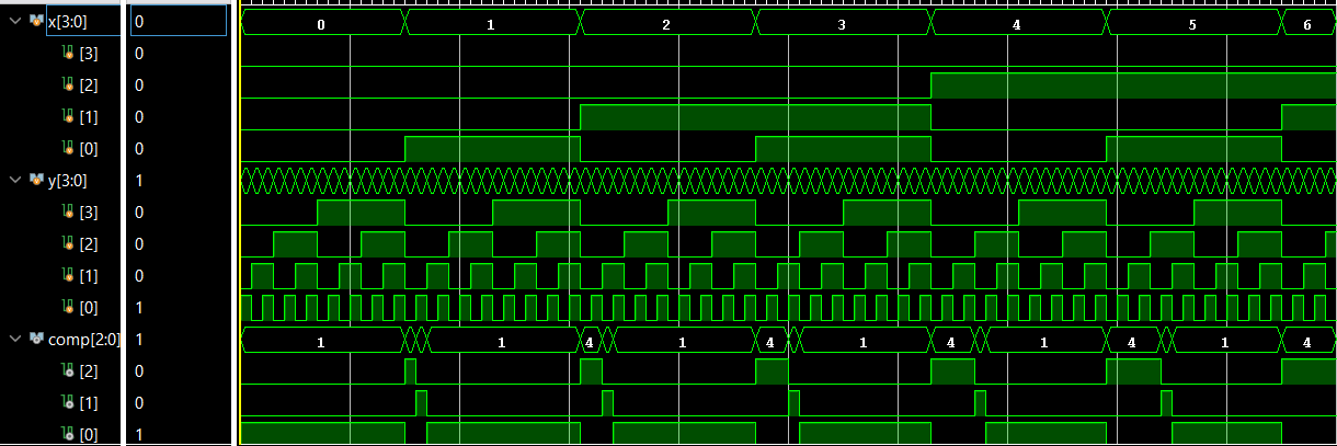
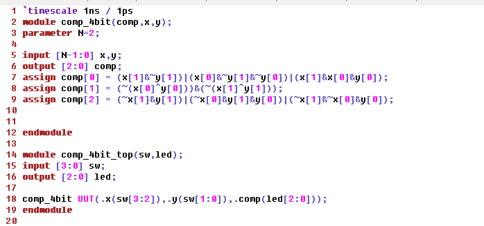
Task 3: 4 bit comparator(10 points).
Figure 3-1: 4 bit comparator code in Gvim
To create a vector, or N bit, comparator the if keyword is used. The
vectors are compared and the comp vector is assigned respectivly. If x
is greater than y as interpreted as a binary number the MSB is one. If
they are equal the middle bit is 1. If x is less than y the LSB is 1
Figure 3-2: 4 bit comparator simulation
Task 4: 2 bit comparator(10 points).
Figure 4-1: Code for 2 bit comparator in Gvim
This comparator is constructed with combinational logic rather than an
if statment and is linked to the 4 rightmost switches on the FPGA and
the three leftmost LEDS. Y is represented by the 2 rightmost switches
and x is represented by the 2 next to y with each having their LSB on
the right. The led output also has it's MSB on the left.
Video 4-1: 2 bit comparator FPGA demonstration
The FPGA boards used in all videos on this report have misinputs form
switches. This is due to the low quality of switches on the board.
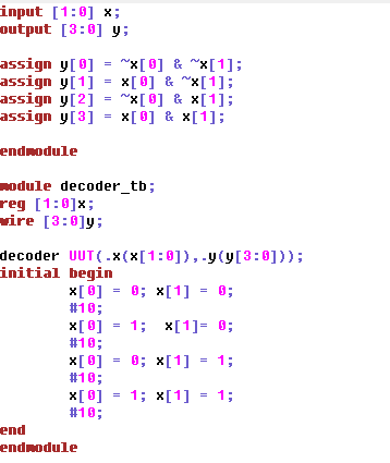
Often in the videos the board will briefly display an incorrect output. Task 5: Decoder(10 points).
Figure 5-1: Code fr Decoder in Gvim
A decoder takes 2 inputs and produces 4 outputs based on the order and
status of the inputs. This decoder can be veiwed as interpriting the
input as binary where x[0] is the LSB and writing a single output to
high depending on the number. 0 being written a 1 when the binary
number input is 0 and 3 being written hign when the input number is 3.
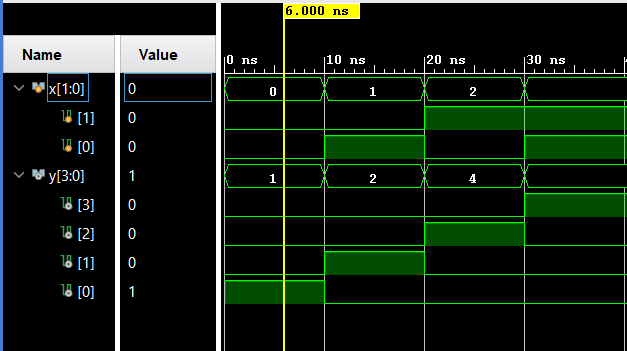
Figure 5-2: Decoder simulation
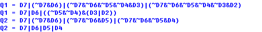
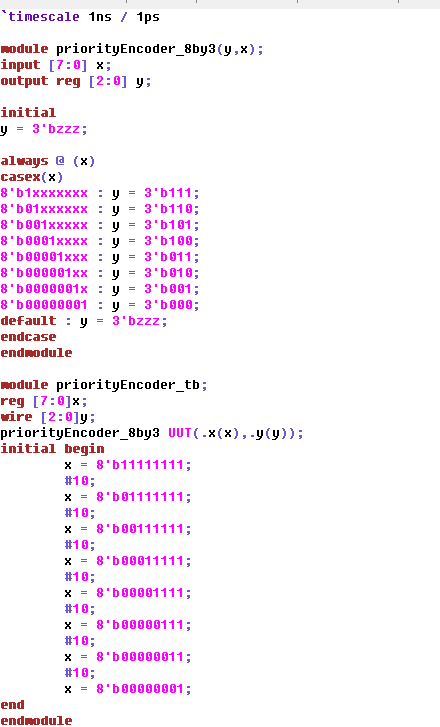
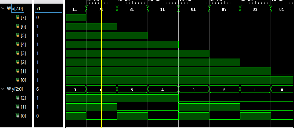
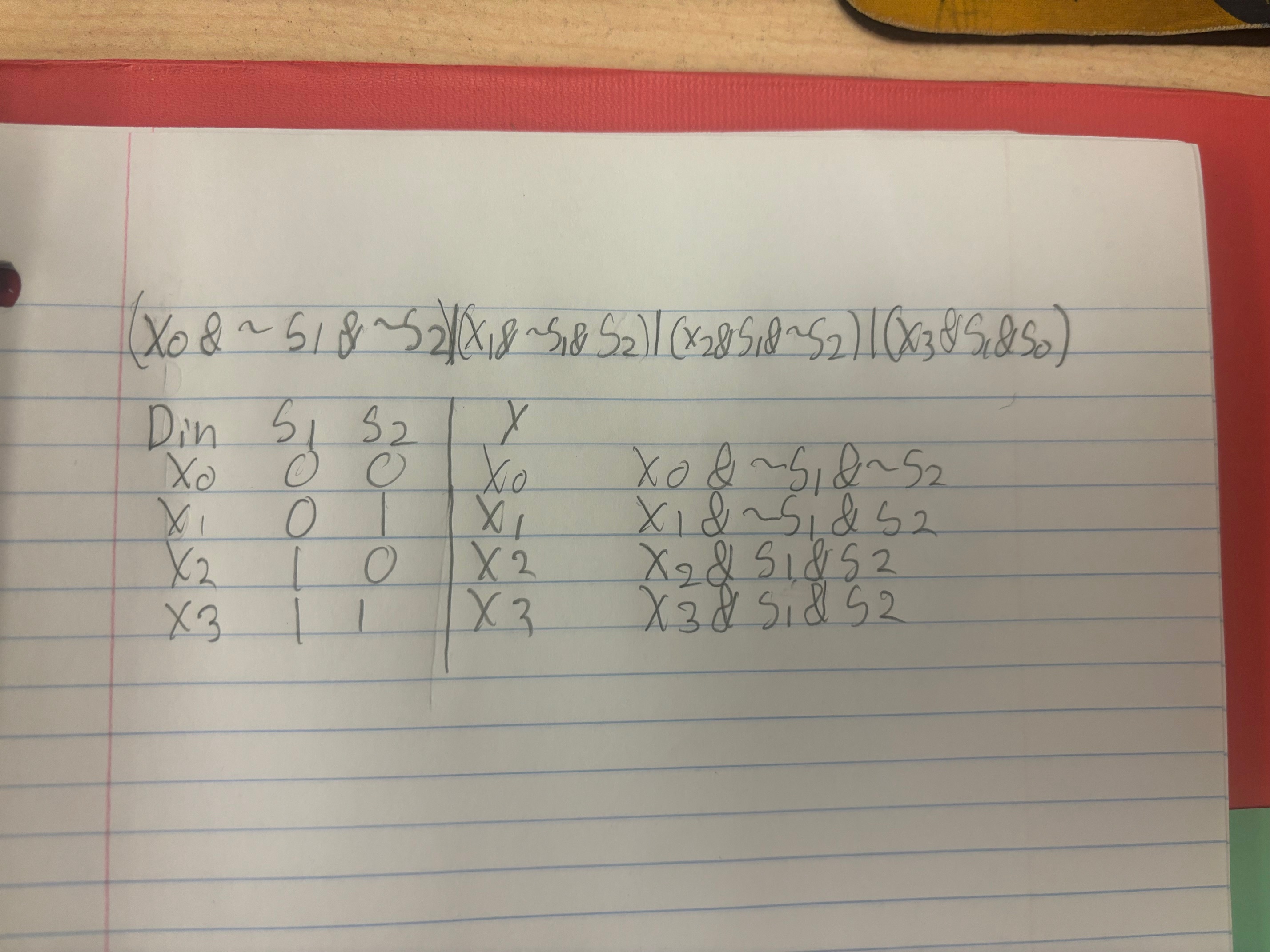
Task 6: 8x3 Priority encoder (10 points).
Figure 6-1: Logic derivation of Q1 and Q2
The truth table of Priority encoder with 3 outputs and 8 inputs yeilds
the following logical expression for the MSB(Q2) and middle bit (Q1).
Figure 6-2: 8x3 priority encoder code in Gvim
Because the inpits have 8 bits and outputs have 3, signifigantly more
inputs can be entered than those who have a spicific output. For his
reason only the most signifigant high bit in the input in considered.
The position of that input is converted to a binary number for the
output using a case statment.
Figure 6-3: 8x3 priority encoder simulation
Task 7: Derive 4-1 MUX logic(10 points).
Figure 7-1: Logic of 4-1 MUX
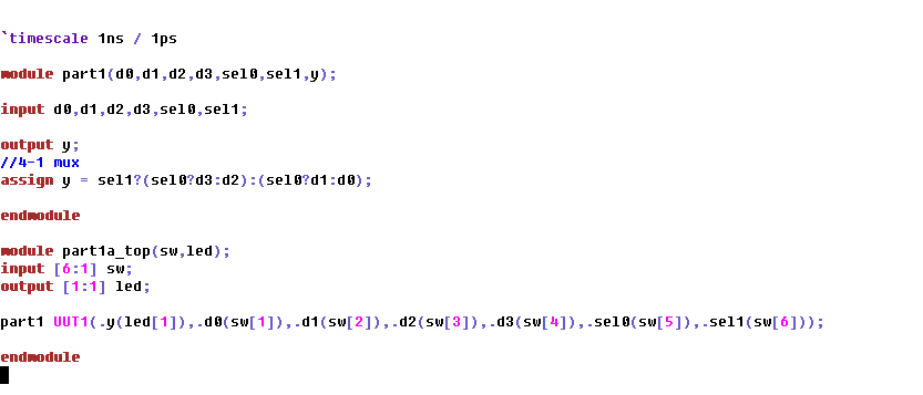
Task 8: 4-1 MUX implimentation(10 points).
Figure 8-1: 4-1 MUX code in Gvim
A MUX uses a selection input to select which of the data inputs is
represented in the output. For a 4 to 1 MUX, 2 selection bits are
needed for a total of 4 possable selection combinations, one for each
of the 4 data inputs. The code for this logic as implimented in Figure
8-1 uses the format: ValToCheck?(valIfTrue:valIfFalse). For
example, if Sel1 is true and Sel0 is false, d2 is assigned to the
output.
Video 8-1: 4-1 MUX demonstration
The first LED is on because an inverter is implimented between switch
one and LED 1.
Task 9: Parity checker and
generator(10 points).
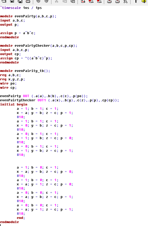
Figure 9-1: Even pairty generator and checker code in Gvim
The even paririty generator generates a 1 for P if the number of high
inputs is odd. This is accomplished with xor logic. The pairity checker
adds the number of high inputs as well as the value of p recieved. If
iven it displays a 1 if odd a 0. A zero would mean data was lost in
translation between the checker and generator.
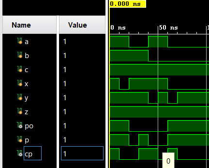
Figure 9-2: Even pairty simulation results
This simulation shows that when an odd or even number of high inputs is
consistant between the generator and checker, check priority (cp) is
high. When the data between the two is inconsistant cp is low. Not all
possabl combinations of logic are shown due to complexity and
redundency.
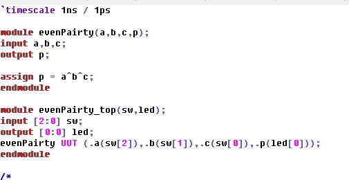
Figure 9-3: Code to impliment pairty checker on FPGA
Video 9-1: Pairty checker on FPGA demonstration
This demonstration is more representitive of a pairty generator as it
is not recieving a pairty bit but rather calculating it. To make a
pairty checker on the FPGA, a pairty generator would also need to me
made. To do this on an FPGA doesnt really make sense because it would
basically be 2 logical blocks doing the same function as a bit would
never be incorrect. So, the program shown in the video was implimented.
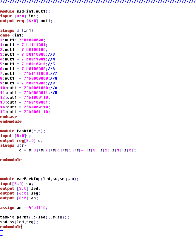
Task 10: Home alarm and counter
with SSD(10 points).
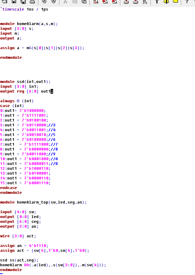
Figure 10-1: Code for improved home alarm system with SSD
When armed, the alarm system desplays an A on the ssd, when not armed
it displayes a 0. This is acomplished with the the case statment is the
ssd module. All but the far right ssd is off so an is 1110.
Video 10-1: Demonstration of improved home alarm system
Figure 10-2: Code for improved counter with SSD in Gvim
The count of bars is displayed on the ssd. This uses the same ssd
module to set the display based on the number of switches flipped
(0-9). Again, an is 1110 because only the far right section is used.
Video 10-2: Improved counter demonstration
Conclusion: This homework sucessfully taught more complex combinational
logic as well as introducing the SSD