ENGR 338 - Course Project 2023 Fall
Name: Ian Van Horn
Email: imvanhorn1@gmail.com
Course Project: SAR ADC in Eletric VLSI
This project requires the Eletric VLSI software
Task 1: Create The SAR Block.
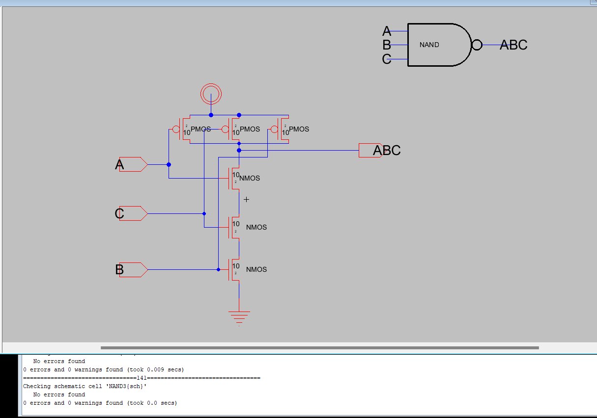
Figure 1: 3 input NAND
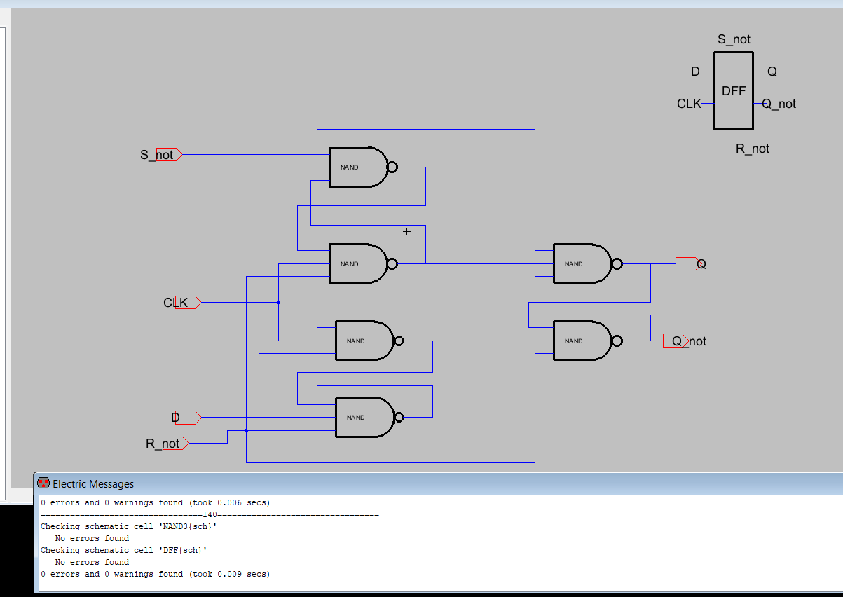
Figure 2. DFF Schematic
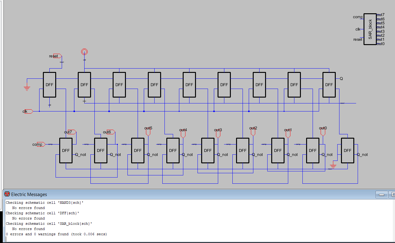
Figure 3: SAR Block Schematic
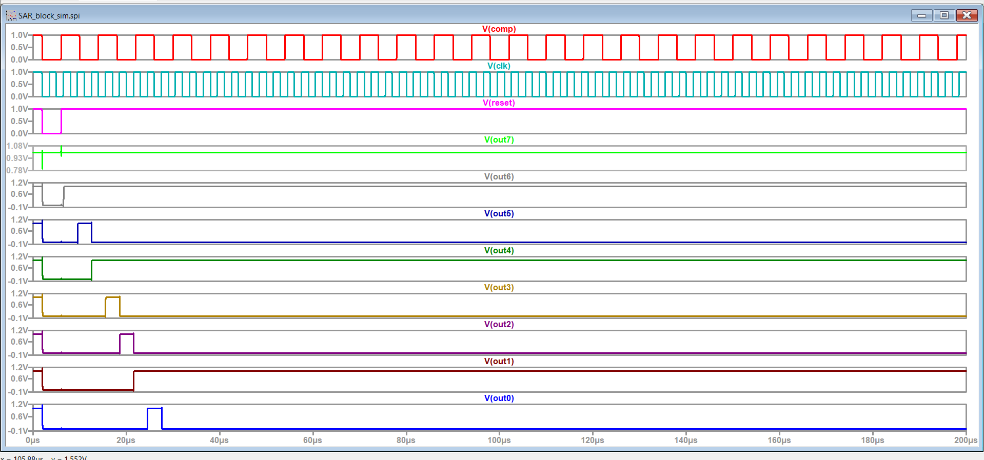
Figure 4: SAR Block Schematic Spice Results
Task 2: S/H and Comparator.
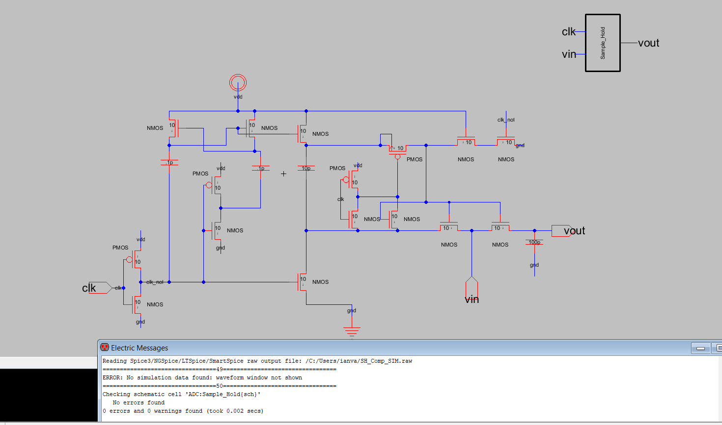
Figure 5: Sample and Hold Schematic
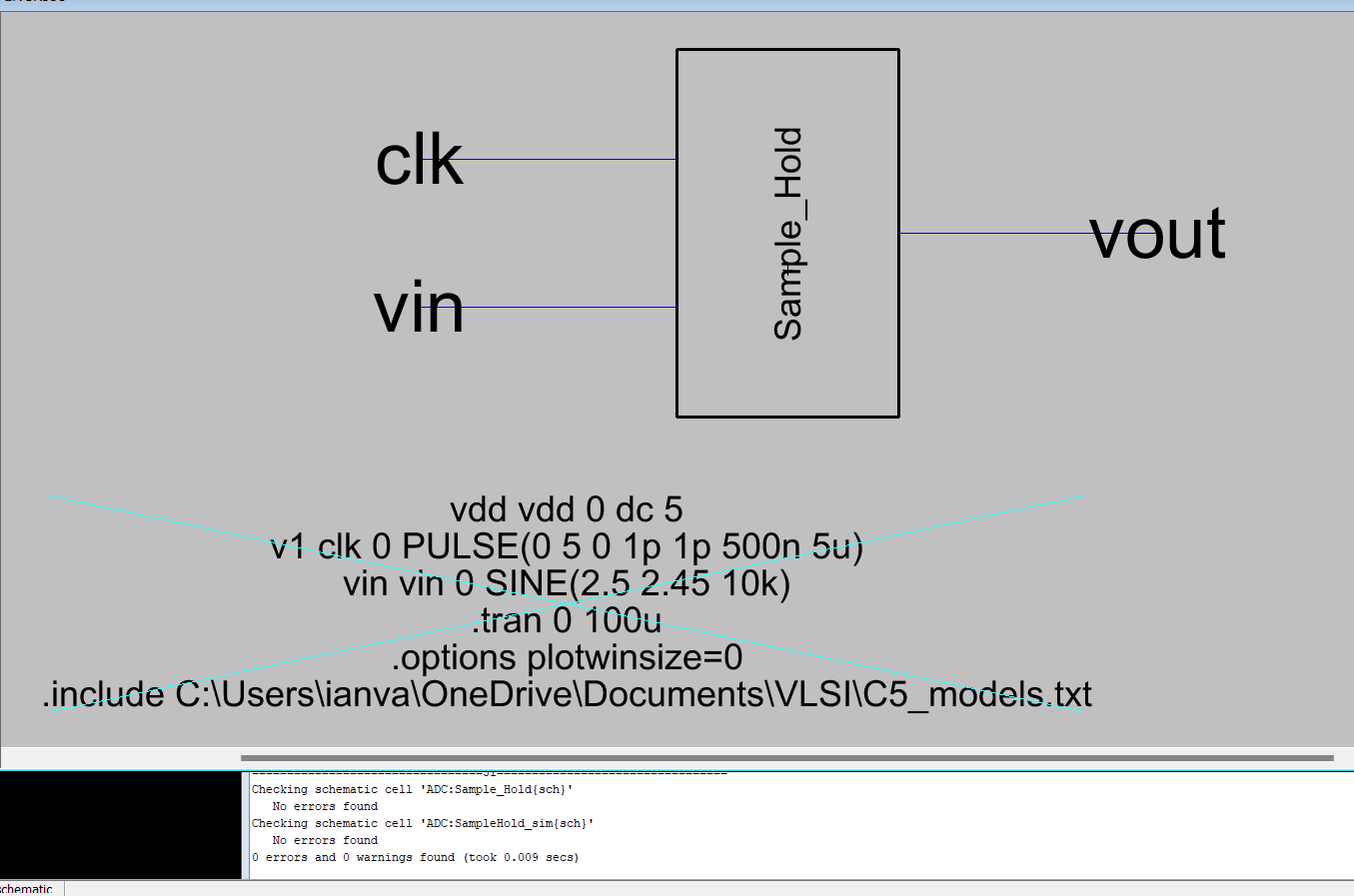
Figure 6: Sanple and Hold simulation schematic
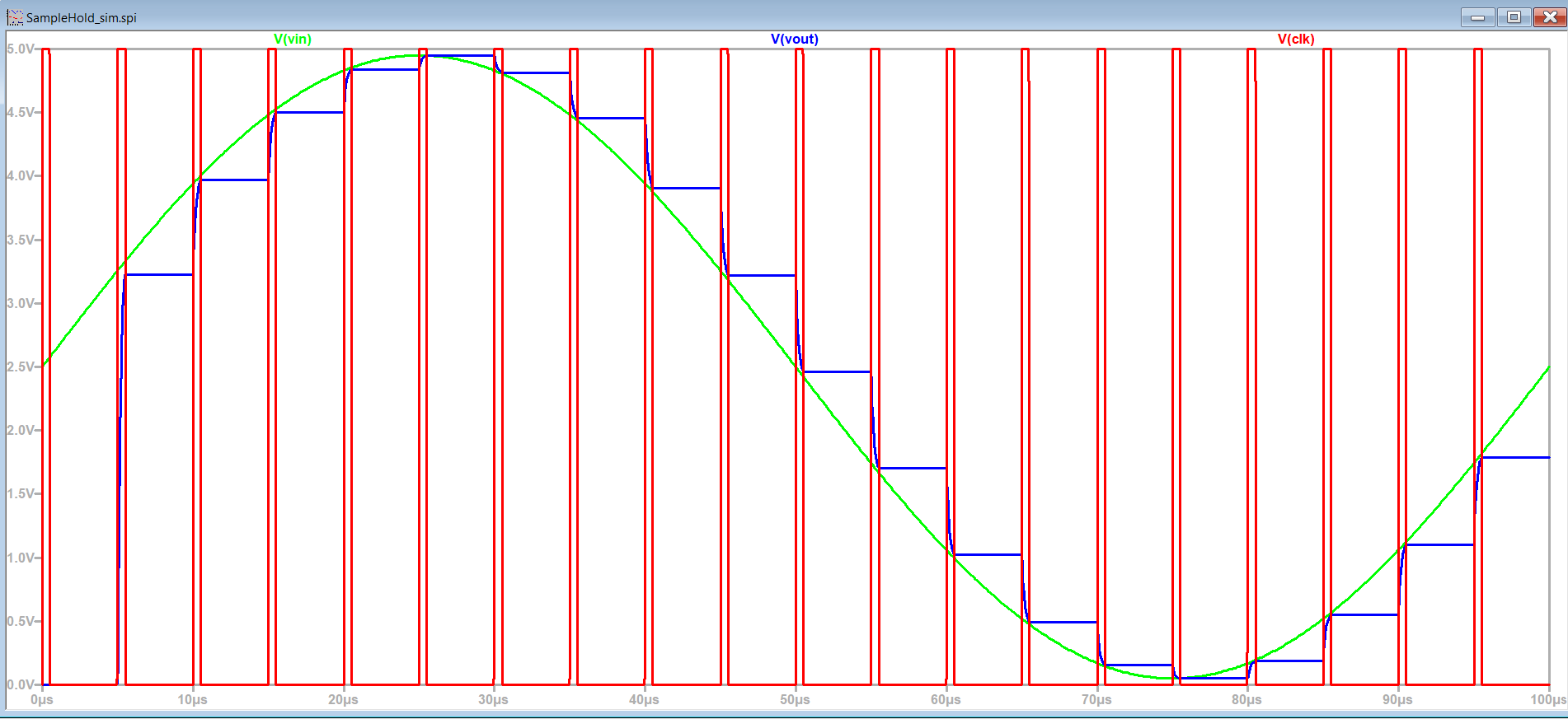
Figure 7: Sample and Hold Spice Results
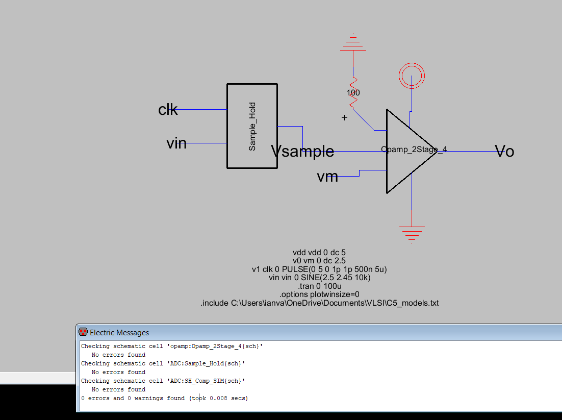
Figure 8: Comparator(OP amp) attached to sample and hold with threshold at 2.5V
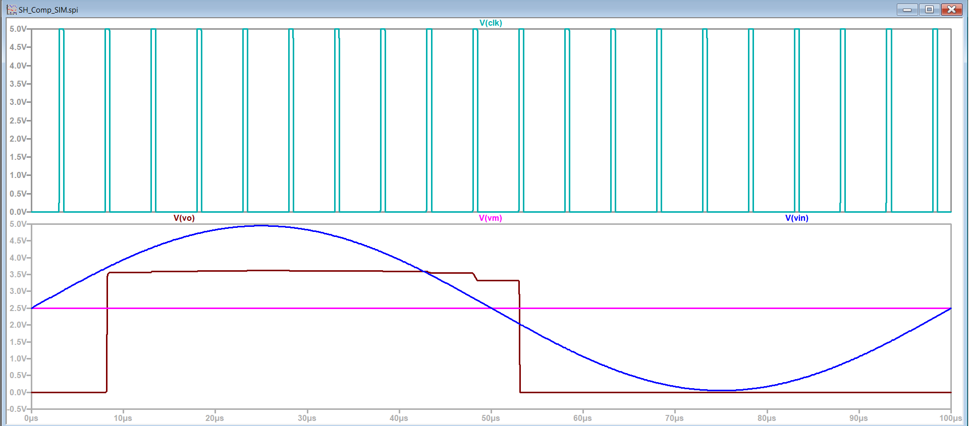
Figure 9: Spice results of Figure 8
Task 3: Compile SAR ADC.
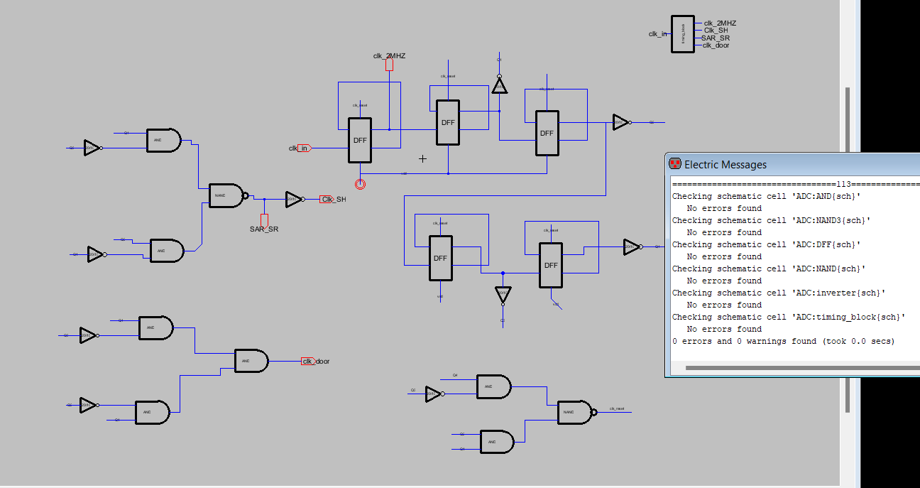
Figure 10: Clock Block
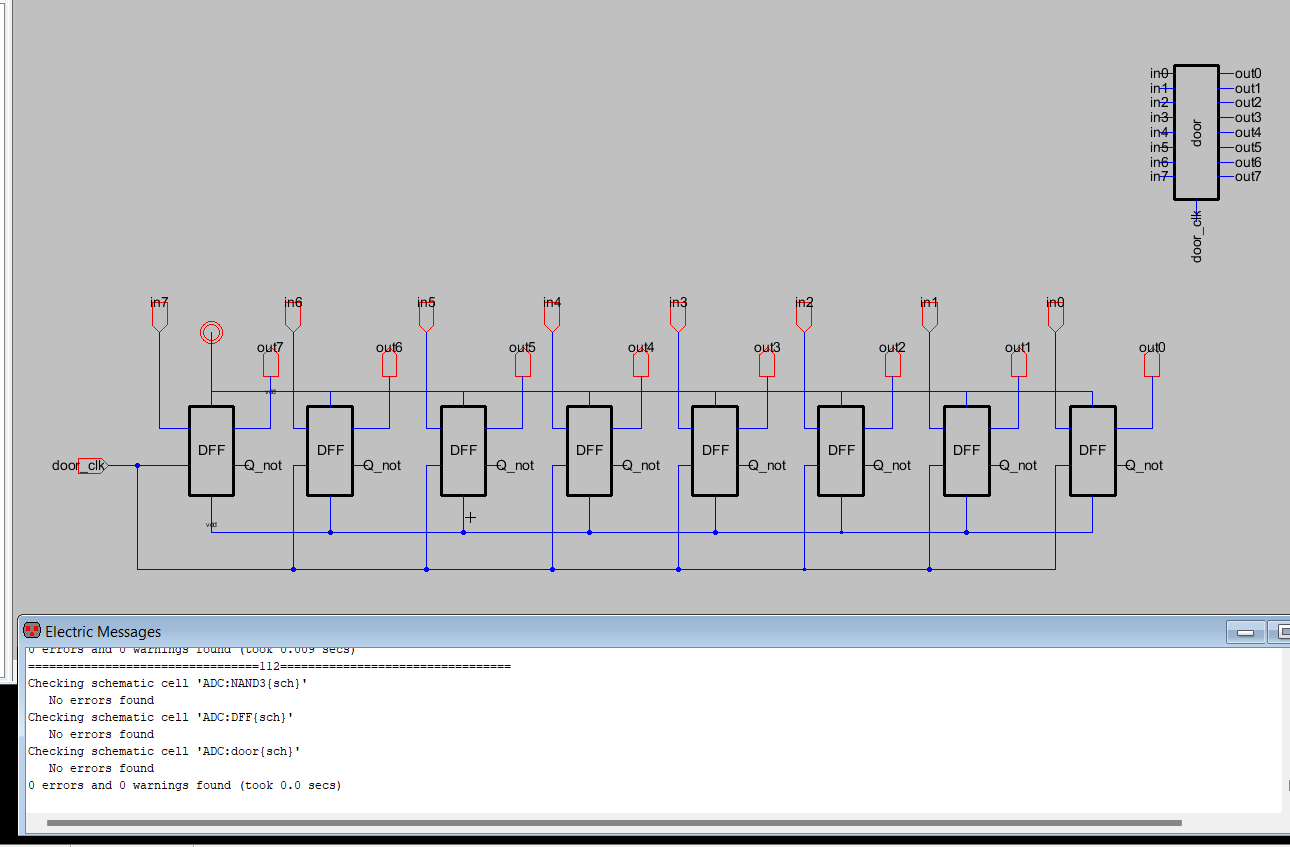
Figure 11: Door Schematic
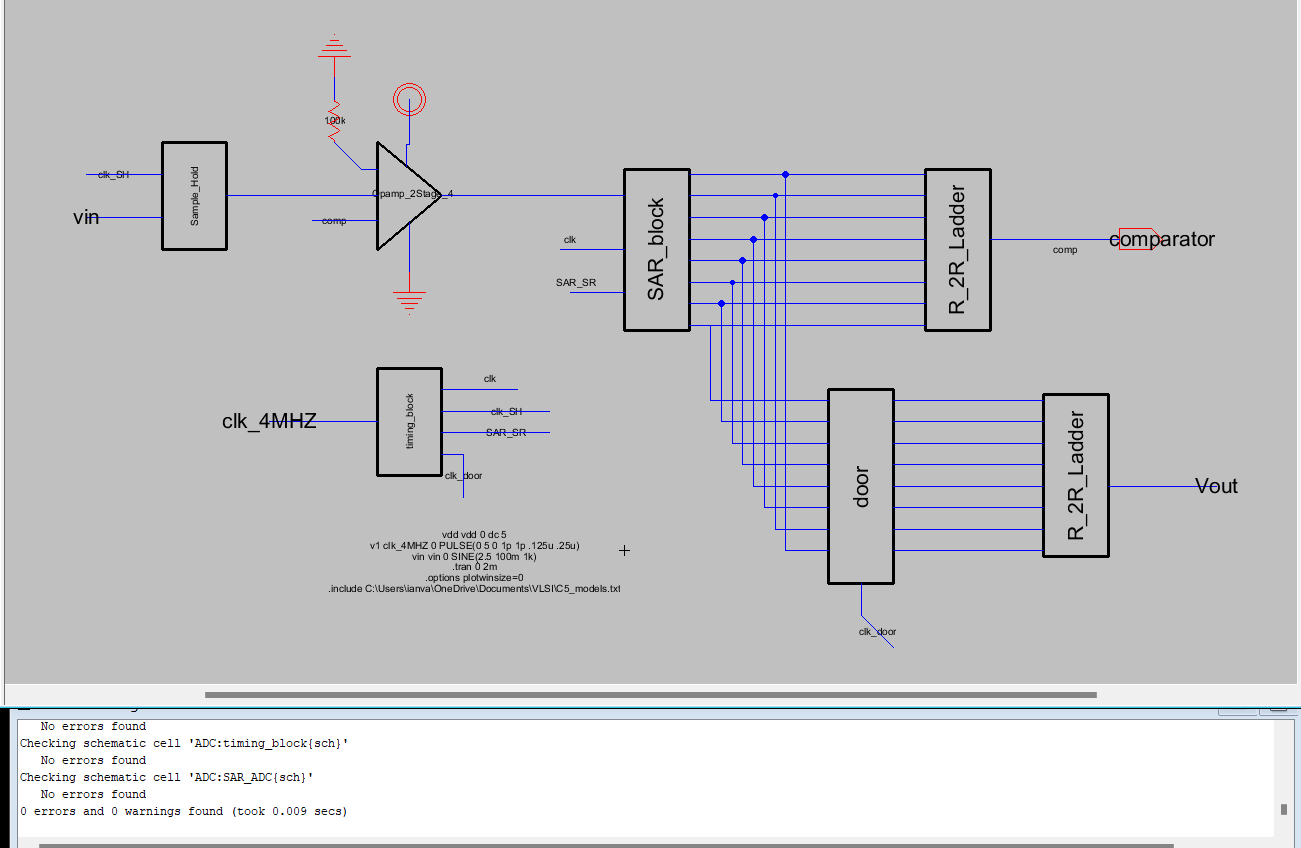
Figure 12: SAR ADC schematic
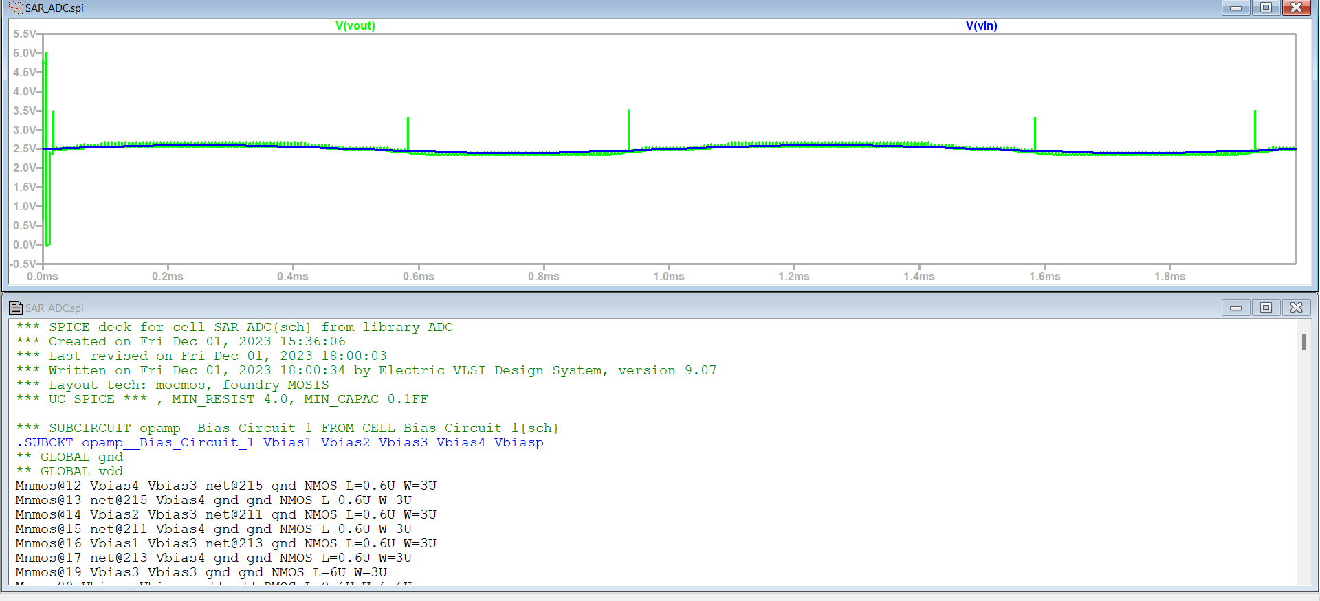
Figure 13: SAR ADC Sine wave conversion
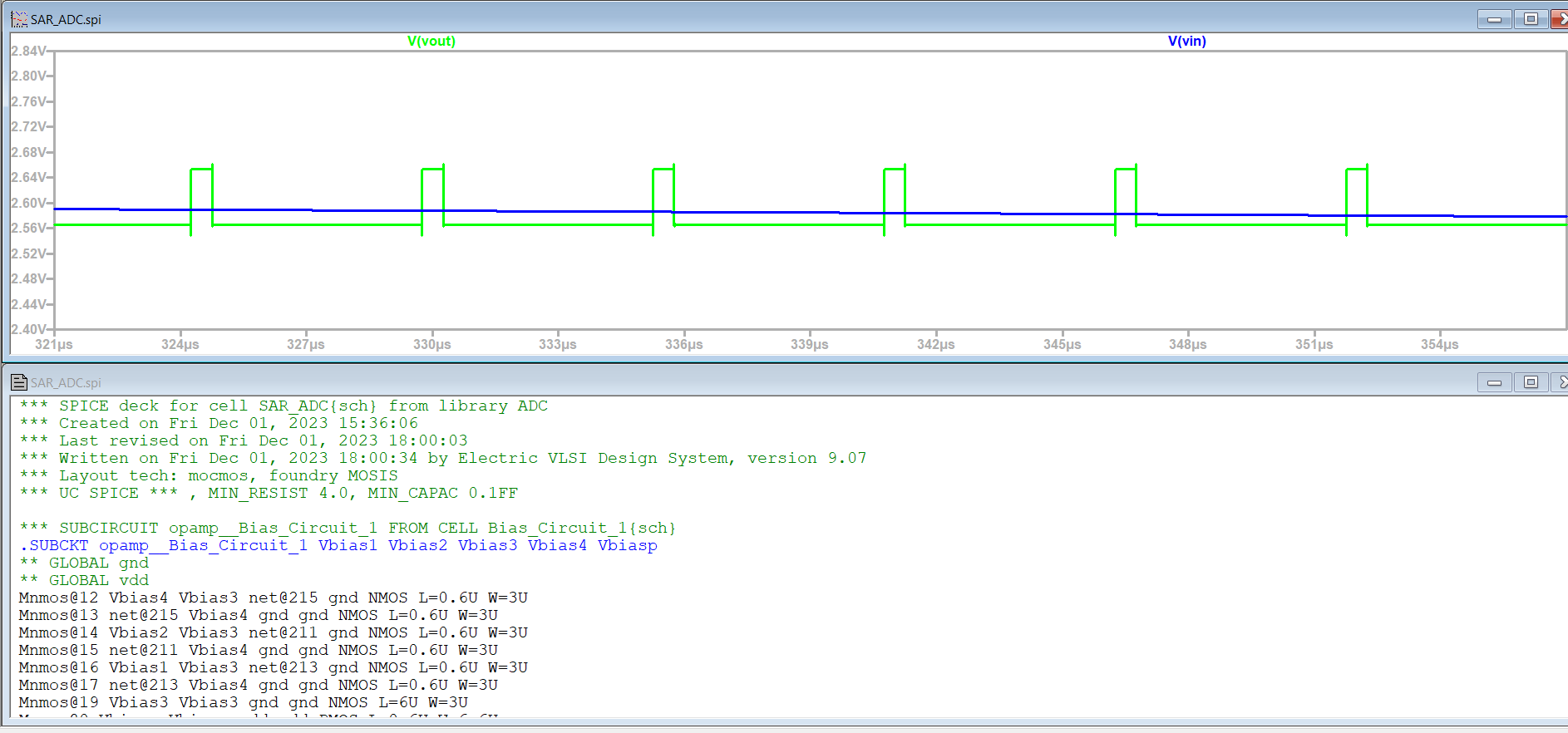
Figure 14: SAR ADC Sine Wave conversion close up
Task 5: Conclusion
The assambly of the ADC helped me more deeply understand how it works.