ENGR 338 - Lab 2023 Fall
Name: Ian Van Horn
Email: imvanhorn1@gmail.com
Lab 7: Using Busses
This lab
introduces busses in eletric VLSI as a way of laying out many gates in series.
This lab requires the Eletric VLSI software
Task 1: Build and simulate a ring ocillator. (20 points).
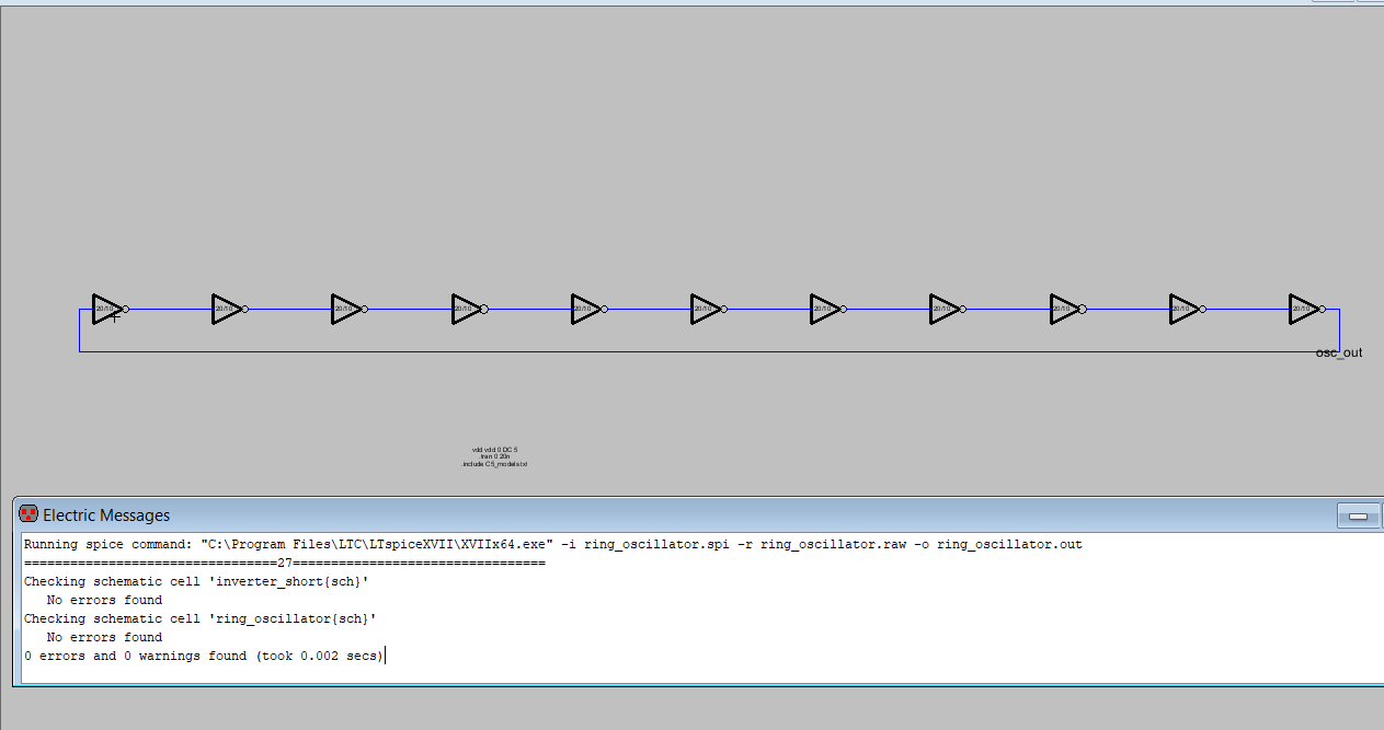
Figure 1:Error free ring ocillator and spice code
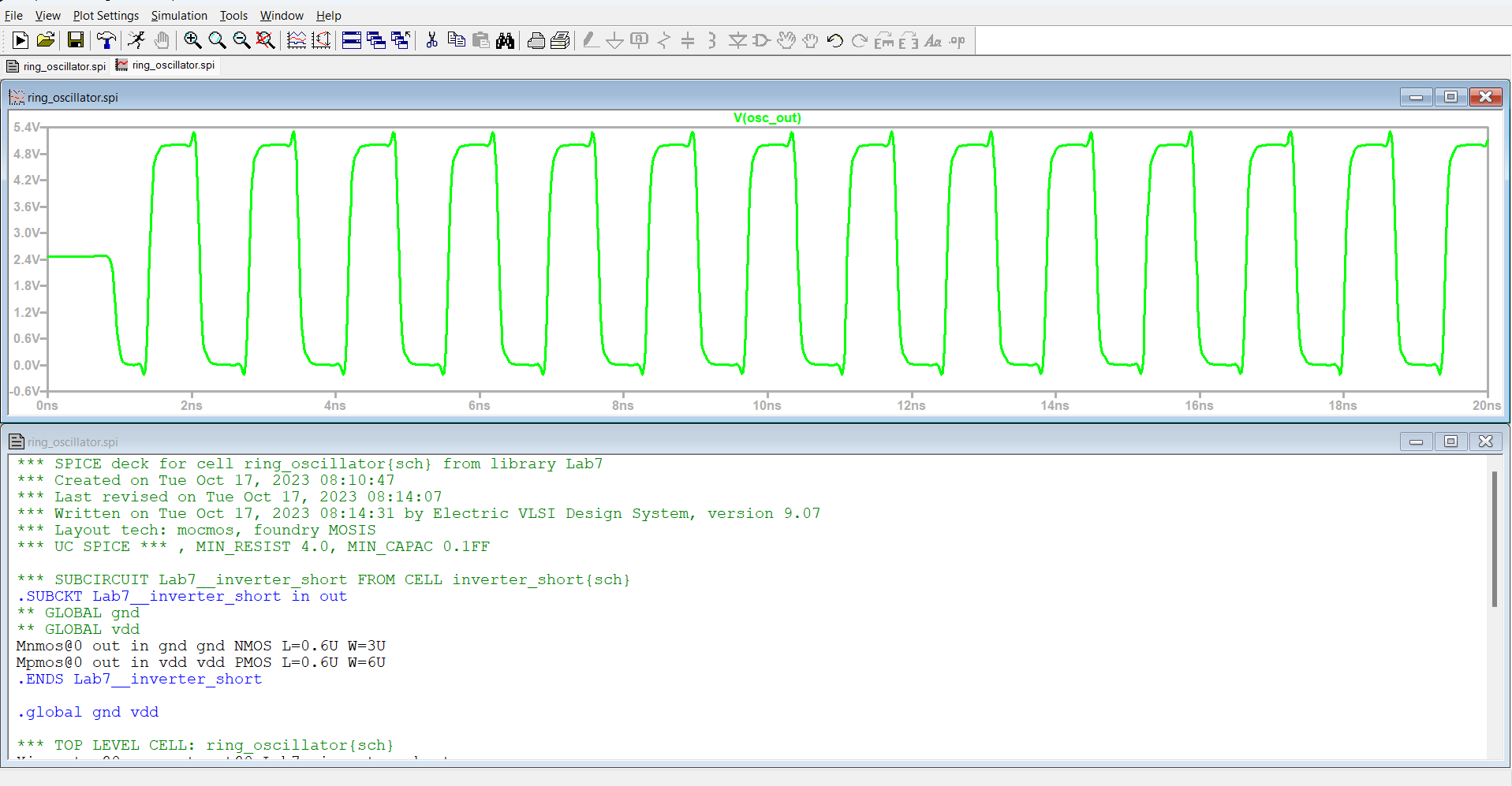
Figure 2. Results of ring ocillator simultaion
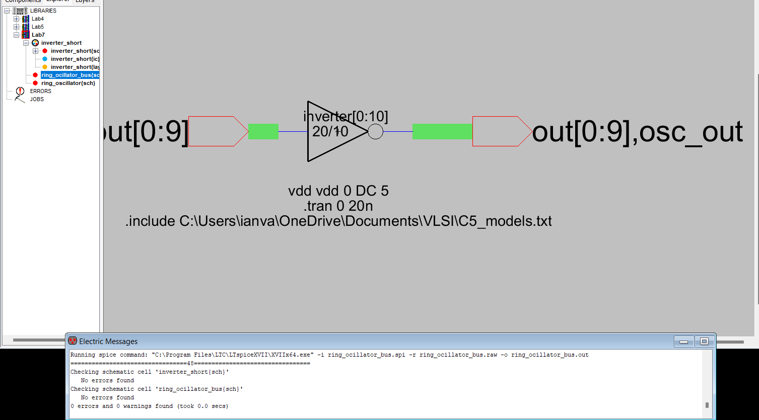
Figure 3: Ring ocillator disigned with busses
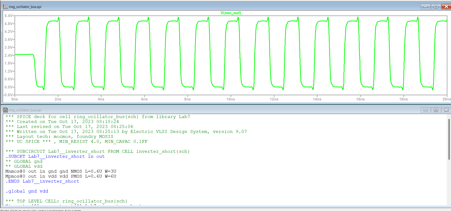
Figure 4: Results of ring ocillator with busses simulation
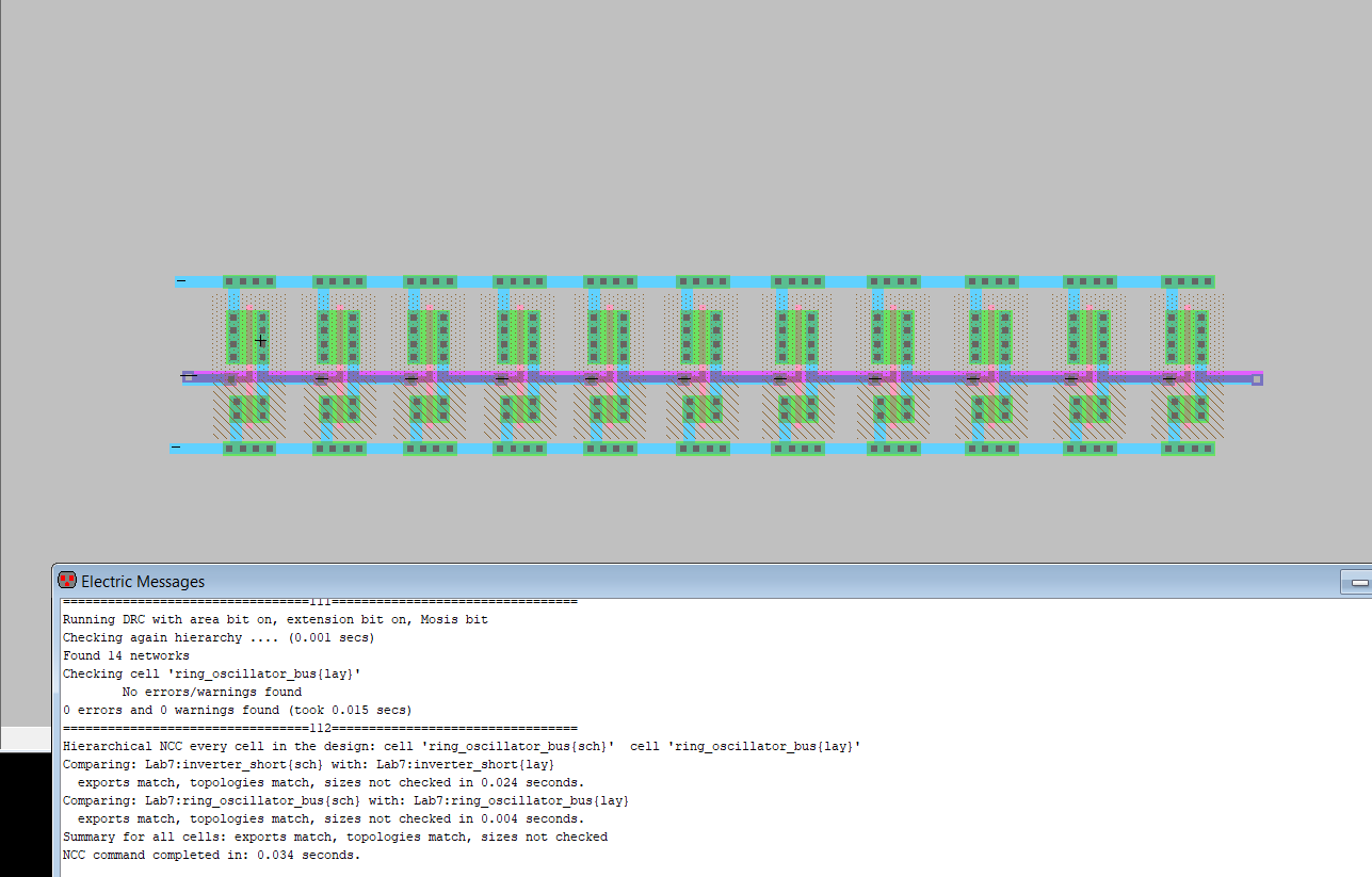
Figure 5: Ring ocillator layout
Busses do not exist in layout. The layout must look how the physical
circut will look. Therefor it does not make sense for busses to exist
in this design step.
Task 2: Design an 8 bit and gate (20 points).
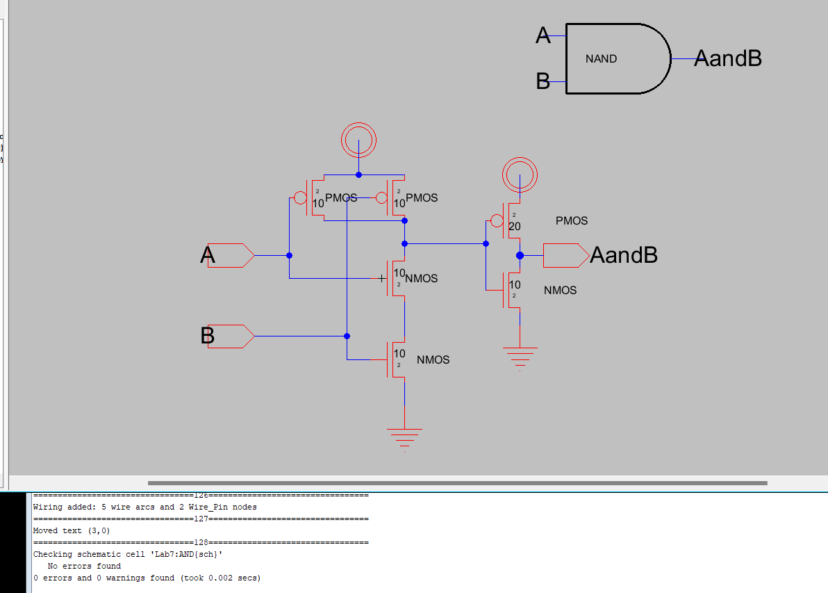
Figure 8: AND gate schematic
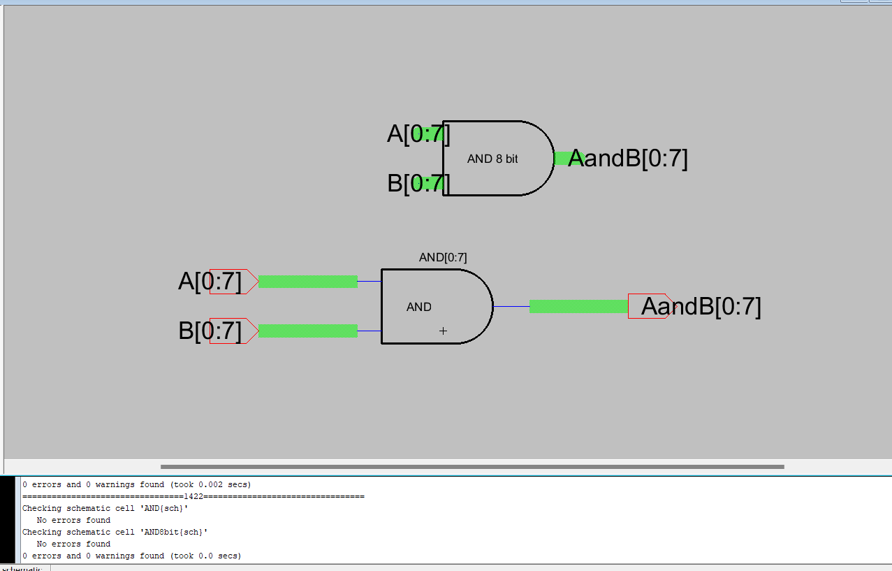
Figure 9: 8 Bit AND gate schematic
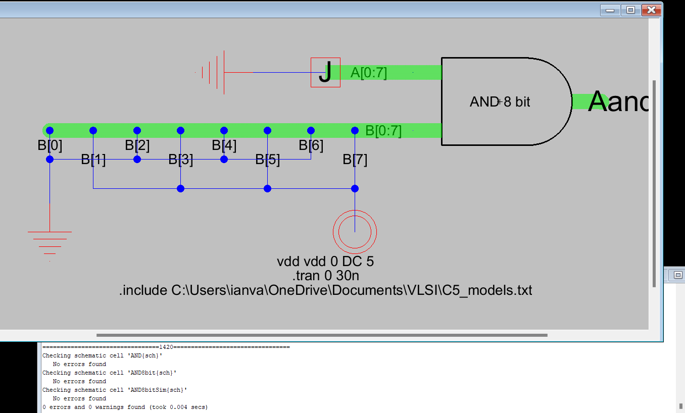
Figure 8: 8 Bit AND simulation schematic
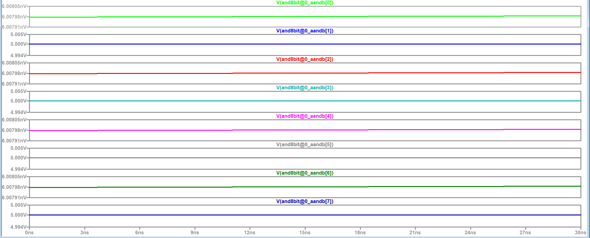
Figure 9: 8 Bit and simulation spice results
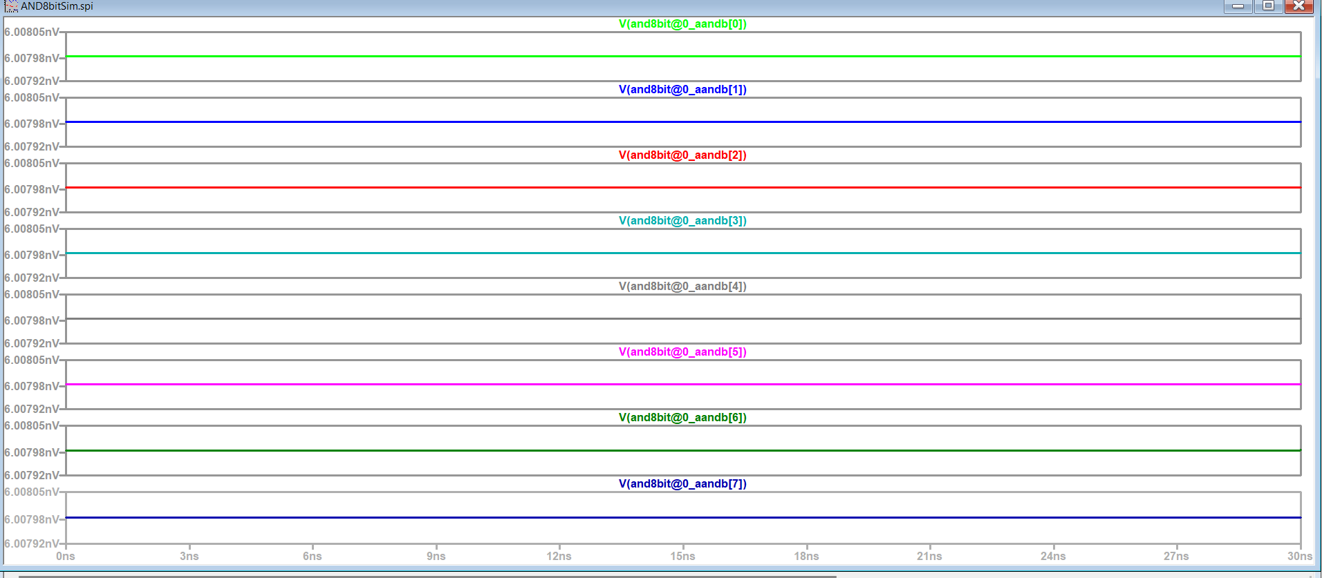
Figure 10: 8 Bit and spice simulation results with input A grounded
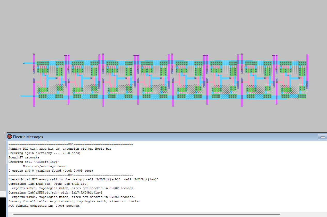
Figure 11: 8 Bit AND layout
Task 3: 8 bit OR Gate (20 points).
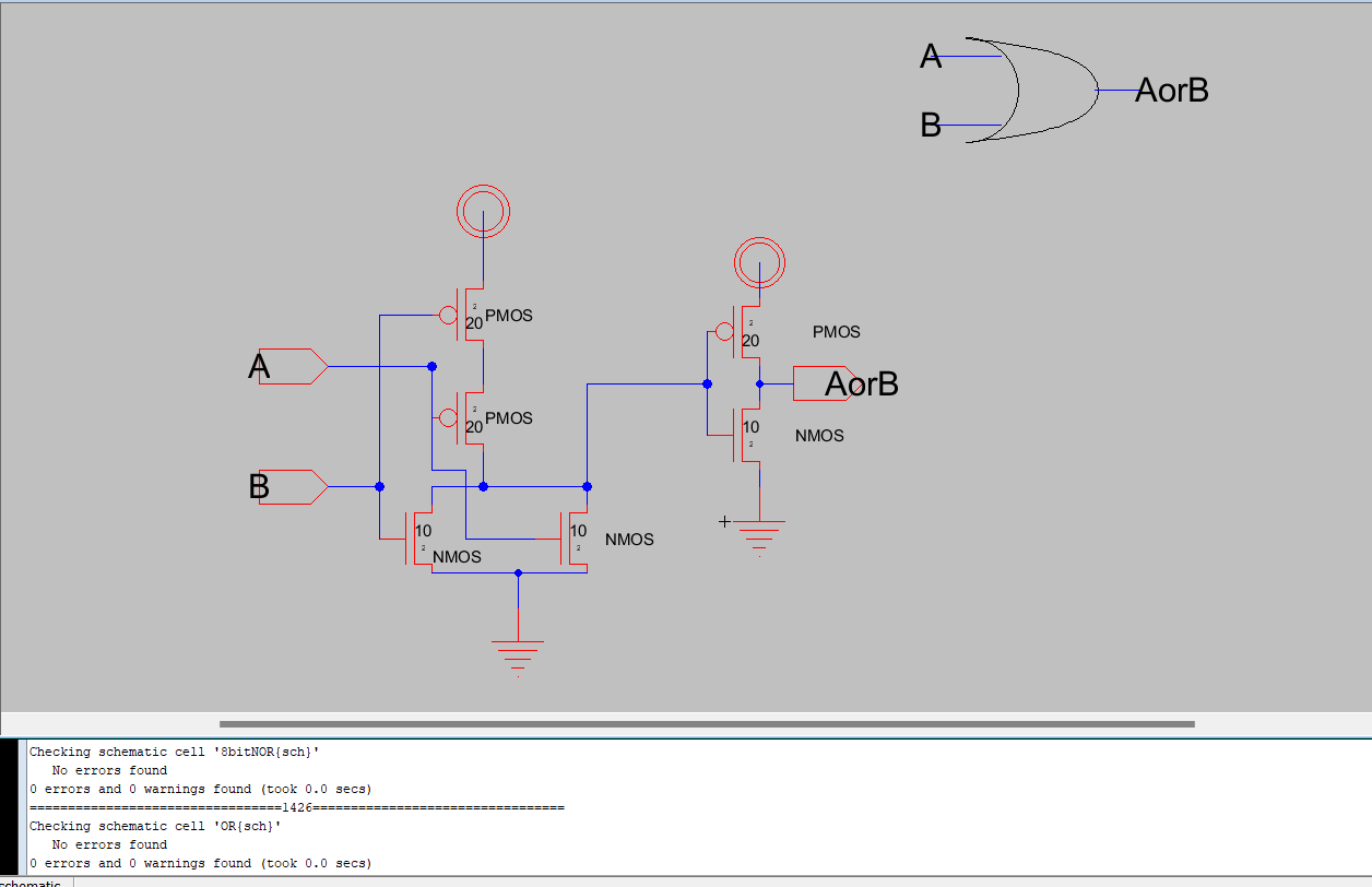
Figure 12: OR gate Schematic
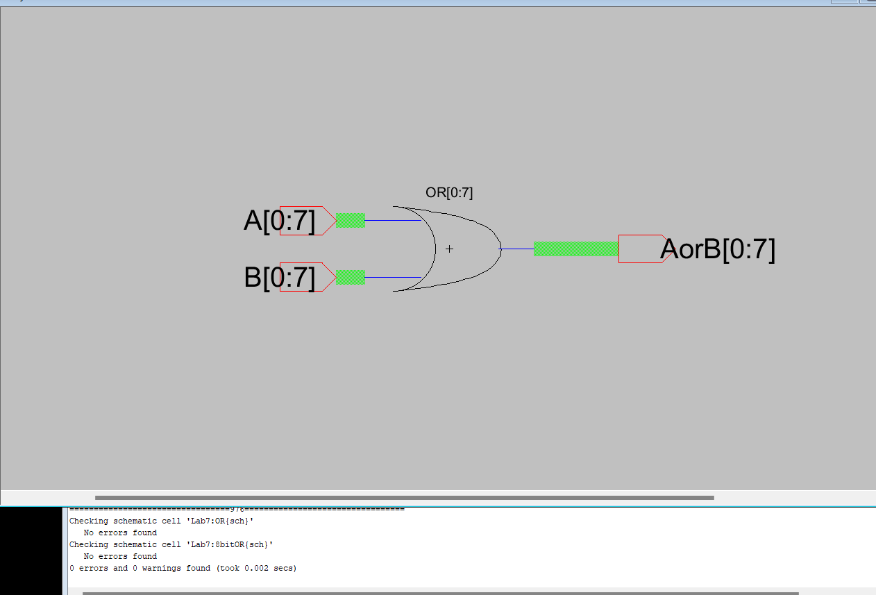
Figure 13: 8 Bit OR Schematic
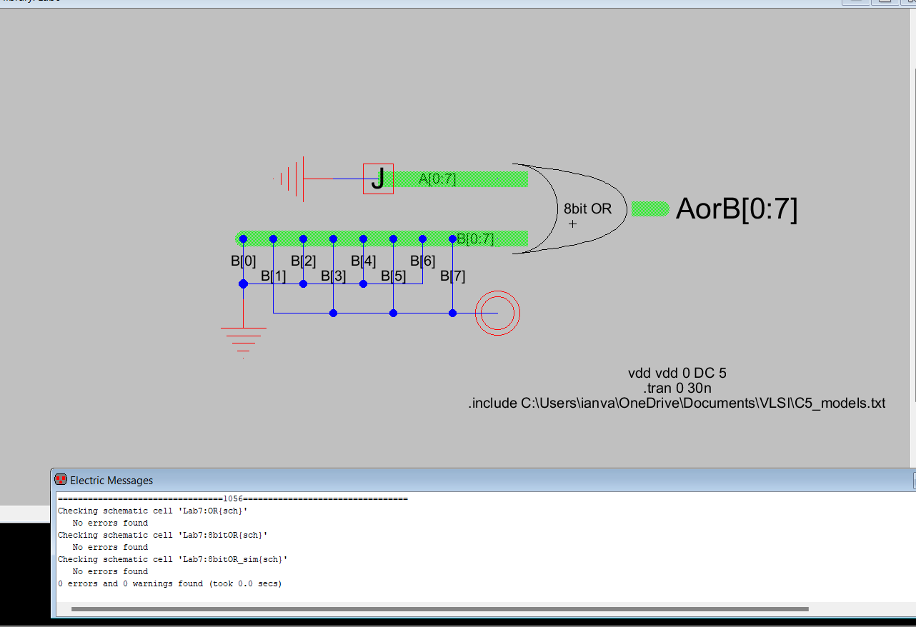
Figure 14: 8 Bit OR simulation schematic

Figure 15: 8 Bit OR SPICE results

Figure 16: 8 Bit OR with input A shorted to Vdd
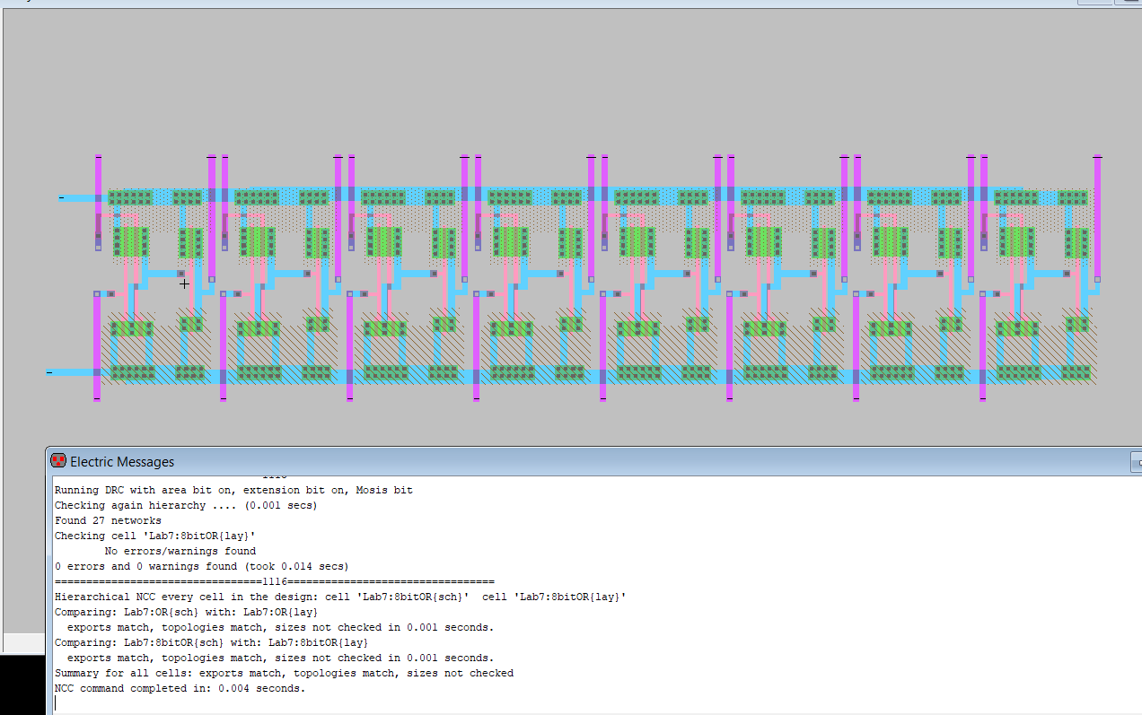
Figure 17:8 Bit OR layout
Task 4: 8 bit NAND Gate (20 points).
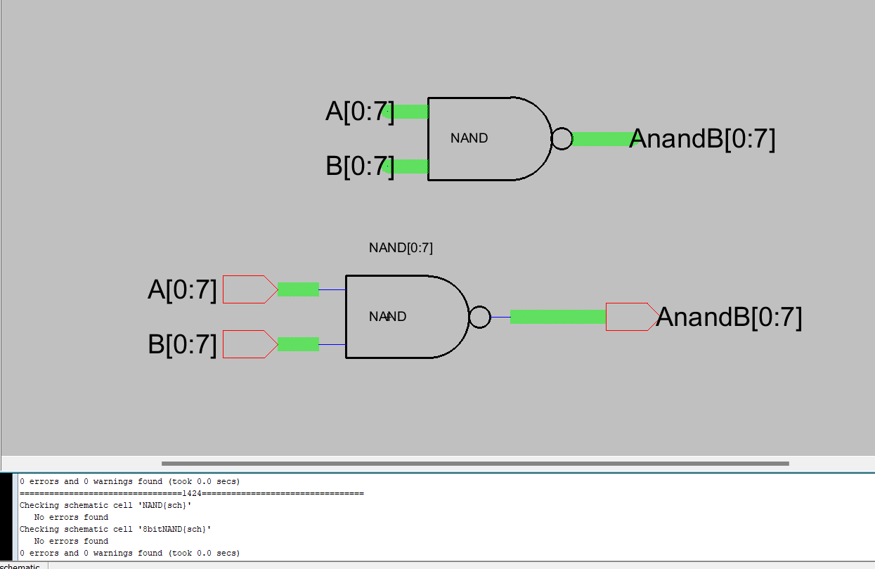
Figure 18: 8 bit NAND schematic
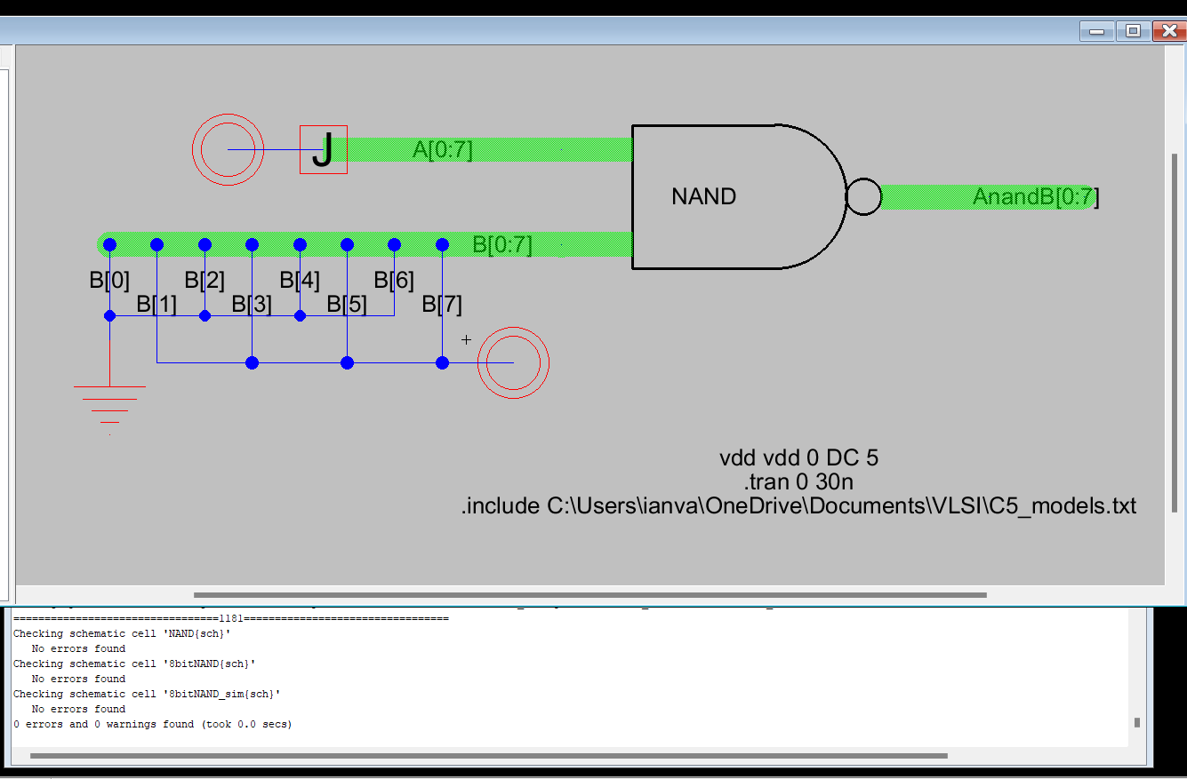
Figure 19: 8 Bit NAND Simulation Schematic
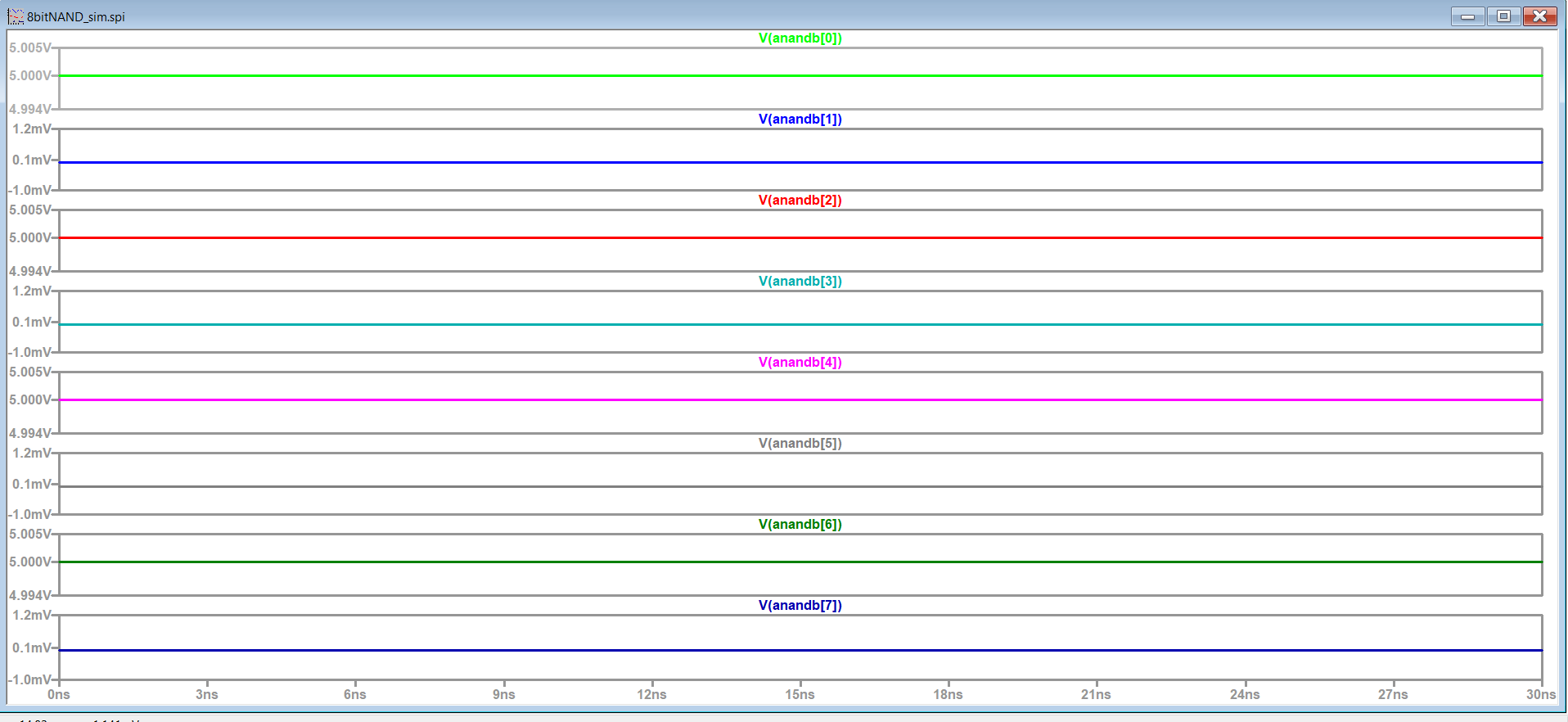
Figure 20: 8 Bit NAND SPICE results
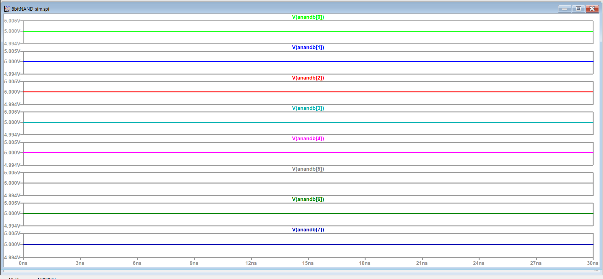
Figure 21: 8 Bit NAND with input A to gnd
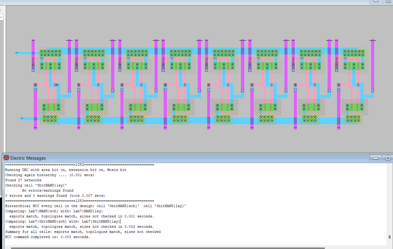
Figure 22: 8 Bit NAND Layout
Task 5: 8 bit NOR Gate (10 points).
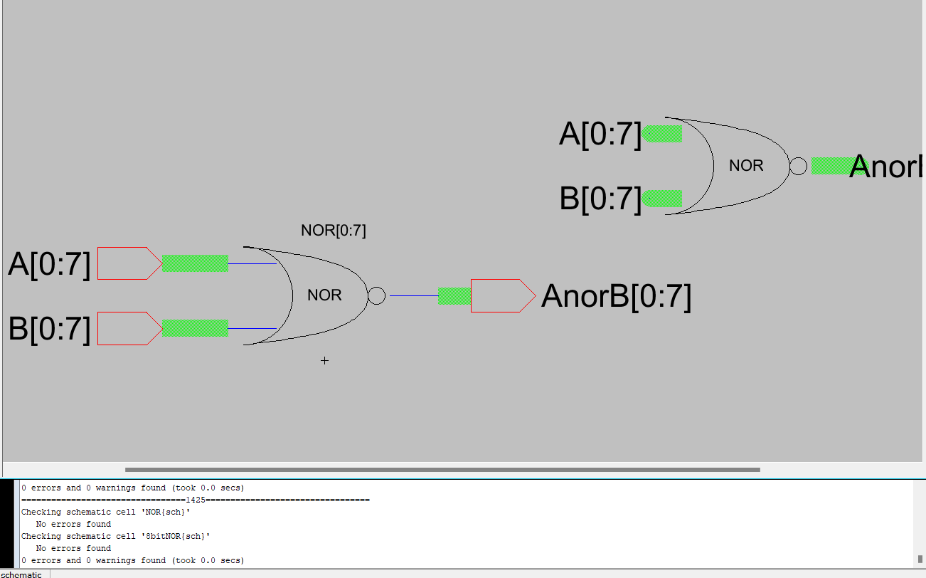
Figure 23: 8 Bit NOR schematic
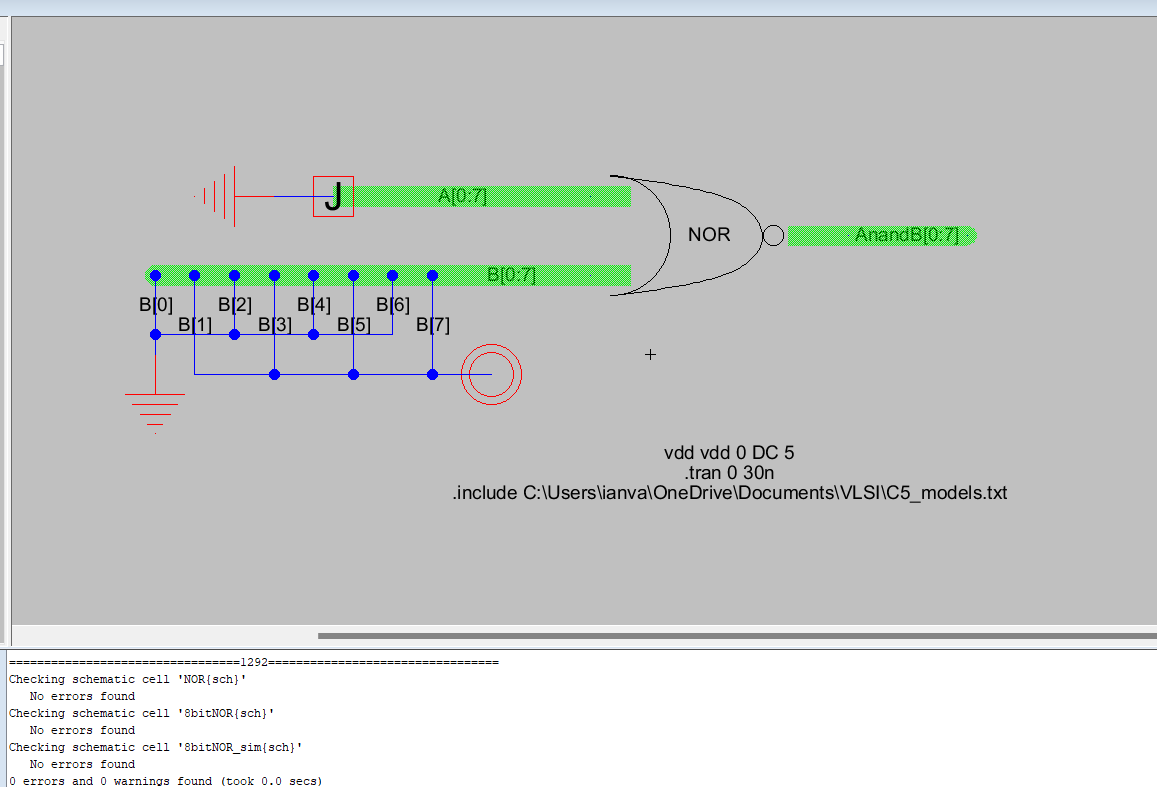
Figure 24: 8 Bit NOR simulation schematic
Figure 25: 8 Bit NOR simulation SPICE results
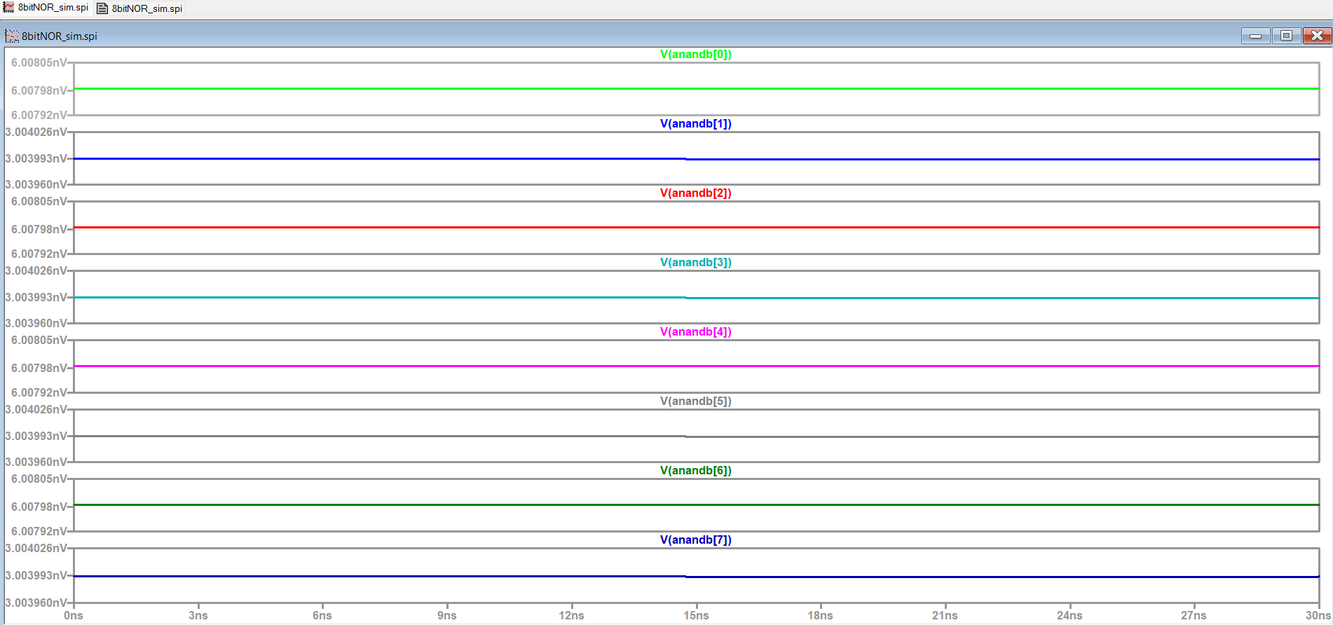
Figure 26: 8 Bit NOR with input A to Vdd
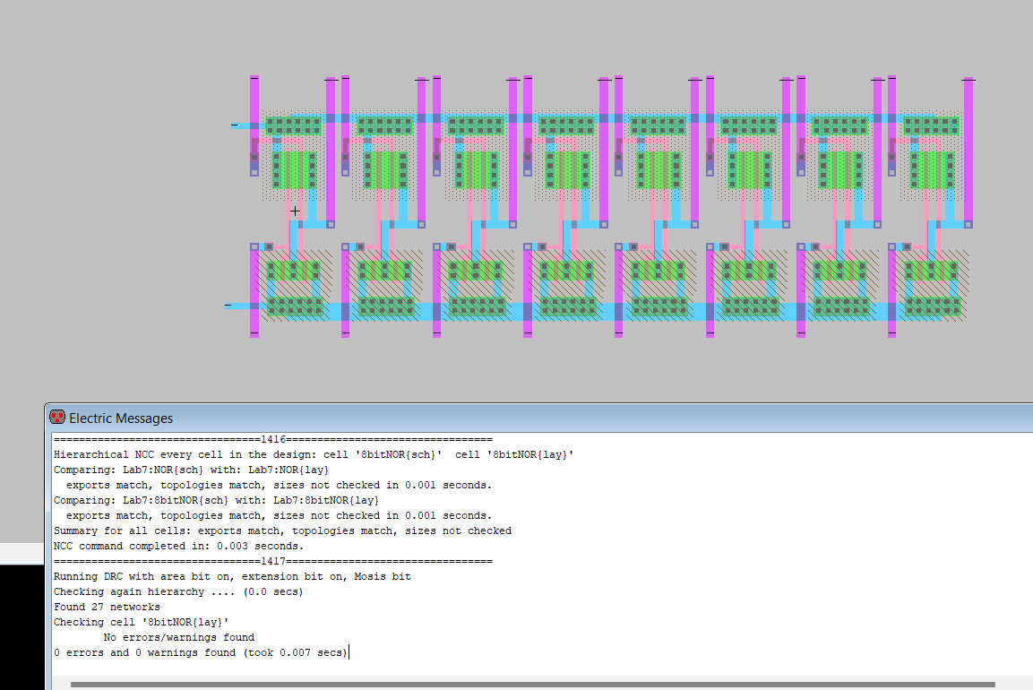
Figure 27: 8 Bit NOR Layout
Conclusion: This lab sucessfully introduced busses