ESP32 Project
Humberto Arredondo
Perez
CE 351 - Fall 2020
harredondoperez@fortlewis.edu
Introduction
For this final project I chose to completed the HW3 all the way to manufacture, solder and test the product.
Methods and Materials
First, in
Figure 1, I created the schematic and layout in Eagle as we did in HW3
following the tutorials provided by Dr. Li. and I must mention that I
had to creaded a couple footprints and symbols for components that
Eagle's Library doesn't have. The voltage regulator design is shown in
Figure 2. Then ,in Figure 3, after we sent out to PCBway out file
in order to get manufacture and we can see how it looks when we recived
it. In Figure 4, we have the final look of the PCB with the components
soldered and after the components are on, its time to load the code.
Finally, In Figure 5 we shown the test results for this product.
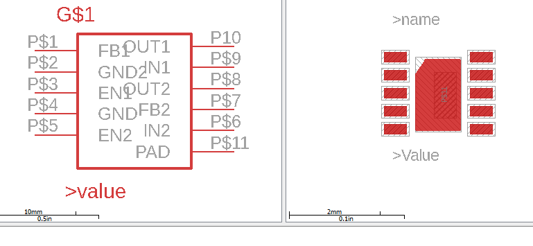
Figure 1. Voltage regulator designed.
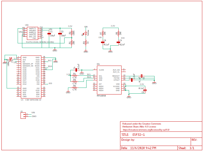
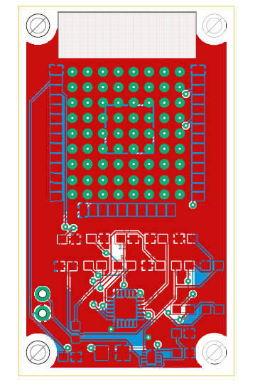
Figure 2. The schematic and layout.
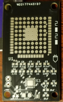
Figure 3. This is how the PCB looked when recieved.
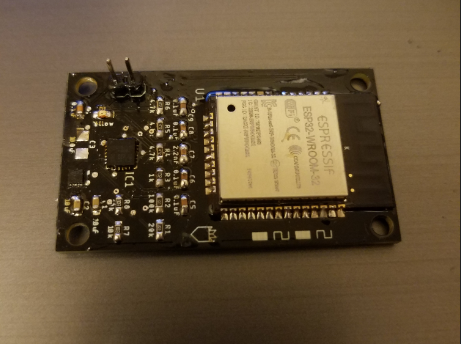
Figure 4. PCB with components.
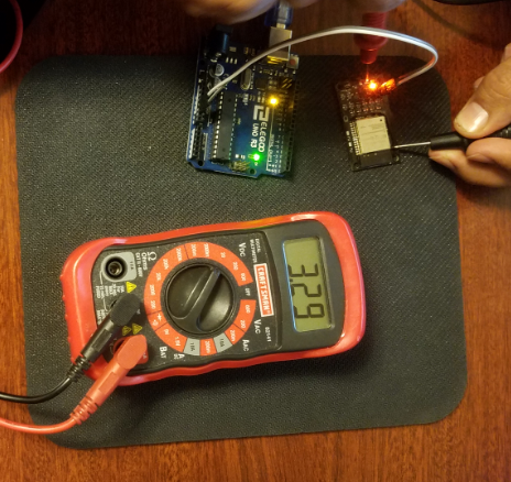
Figure 5. PCB test results.
Discussion
This
lab was fun and challenging. The more we use Eagle that more
issues we found. These isuess became to me more skills to use this
program. we learned some tricks on finding a library for components so
we can save time when developing the schematic. It does take lots of
attention to solder this components, any small error will cause the
board to fail.