ENGR337 Lab 2020 Spring
Lab 8
Name: Humberto
Arredondo Perez
Email:
harredondoperez@fortlewis.edu
1. Title: Layout an inverter
2. Introduction
The goal of this lab was to learn how to do a layout of an inverter using a NMOS IV and PMOS IV transistors in ElectricVLSI by
following the instructions of the tutorial 3.
3. Materials and Methods
In
this lab we used a software call ElectricVLSI and the tutorial 3 given
by
DR Li. We created a new cell for the NMOS and PMOS node that we
had previously designed, we changed the length, changed the nodes to a
transistors. To create the inverter, first, we place the NMOS and
PMOS in a schematic, conecting the drain of pmos to the source of nmos,
the source of pmos to power and the drain of nmos to ground. The Vout
location was in between this to transistors. we did something similar
for the layout while we learned how to do a icon. We ran a simulation
in LTSpice for both cases making sure they both worked.
4. Results
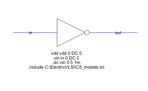
In figure 1,the schematic of the inverter with NMOS and PMOS transistors are showen after
were modified in terms of lenght and names of dimentions
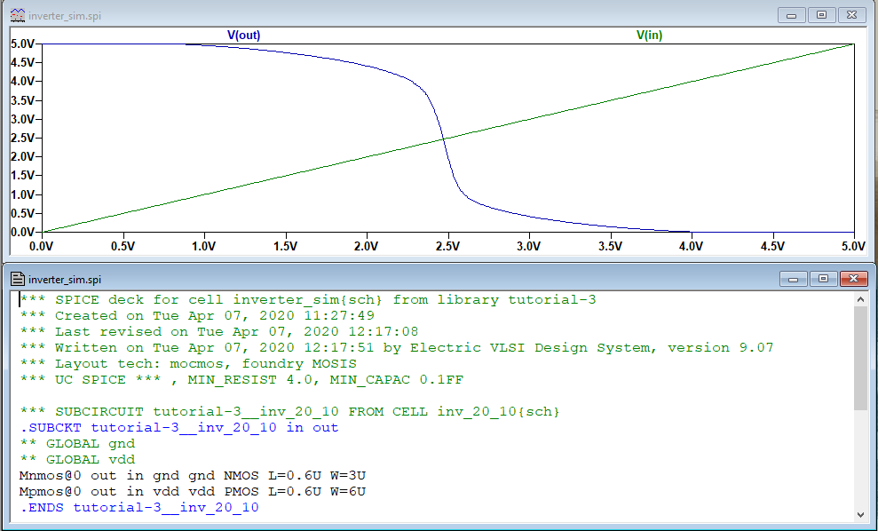
and place a code. In Figure 2 the results of figure 1 are showed from
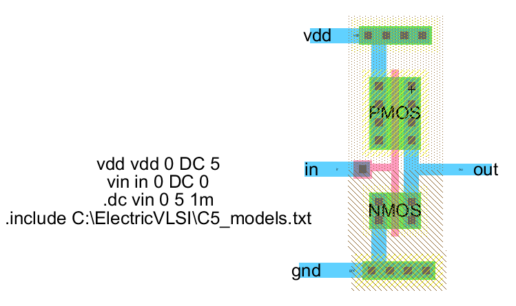
LTSpice. Then we are showing on Figure 3 the layout version of this
inverter.
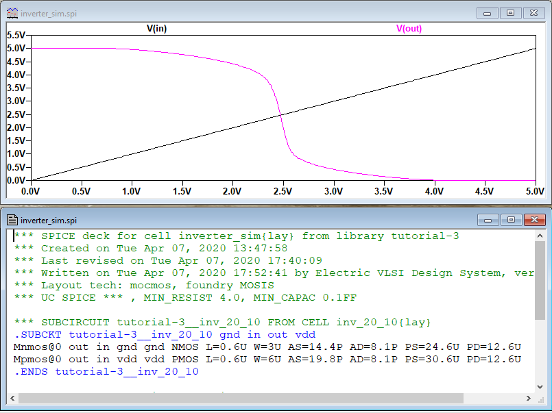
Figure 4 We have the simmulations of Figure 3 squematics
and with the respective code to make them work.
Figure 1 NMOS and PMOS transistors in a inverter schematic form and the icon on the right.
Figure 2 Simulations results from LTSpice.
Figure 3 Layout if the inverter with code.
Figure 4 Layouts ran
in Spice with the code showned
5. Discussion.
In this lab we
got
designed a Invertes using a NMOS and PMOS transistors, create and icon, and refreshed how to
labaled, sized, check for errors, run on Spice. we can see how we obtained the same results on both cases. Great lab 3 of
this series of 6 in total. checking for errors its a powerful tool and time saver when disigning on ElectricVLSI.