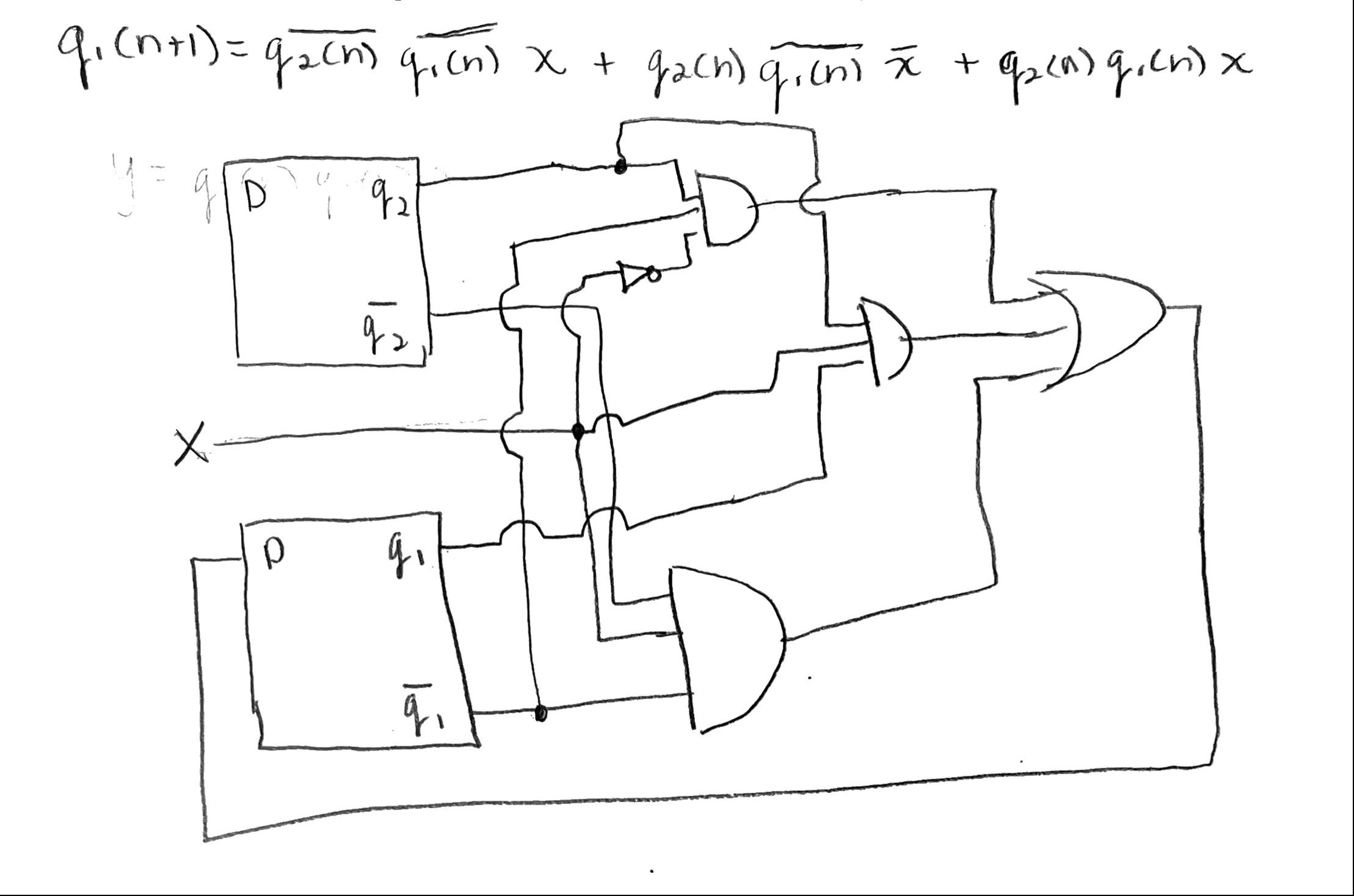
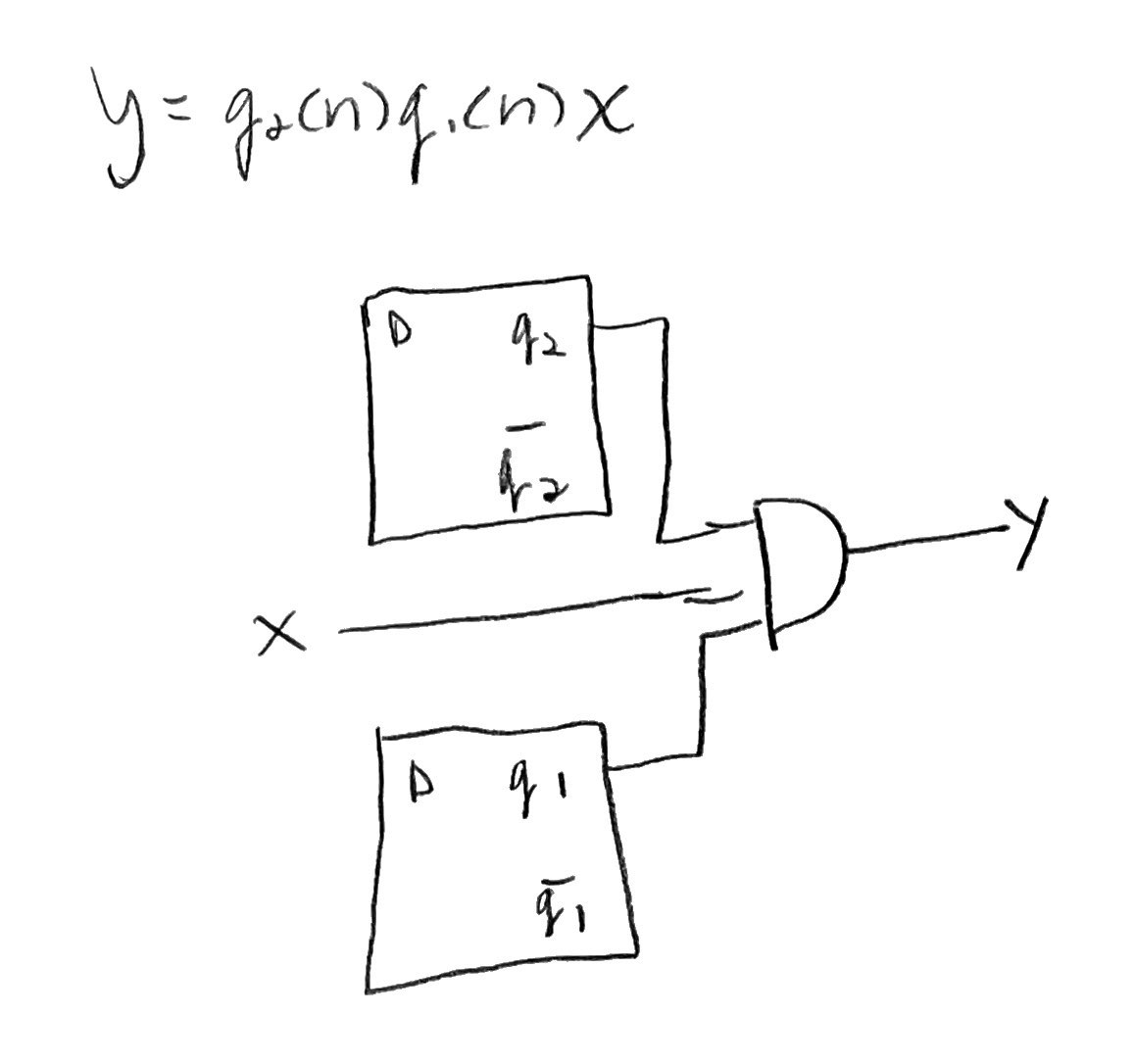
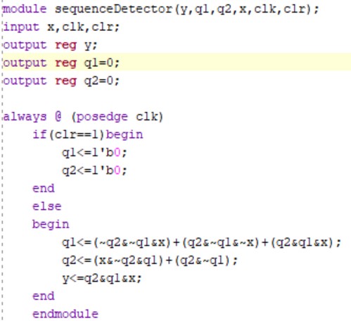
The ouput y is simply y = q2[n]q1[n]x, with no need for a K map.
Task 2 - Repeat the work in Section 3. Use two methods, the given one and the behavioral one. Show simulation results.
Given method.
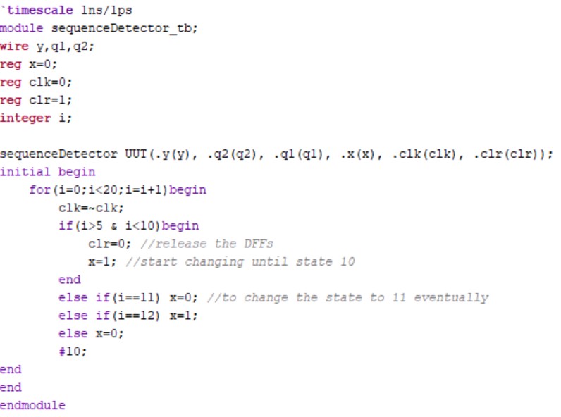
Behavoioral method
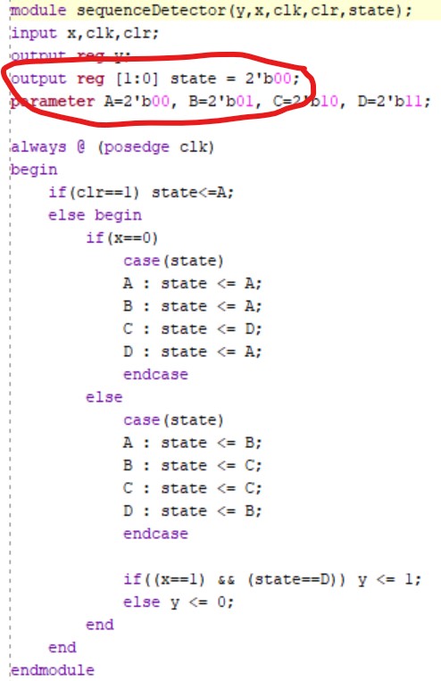
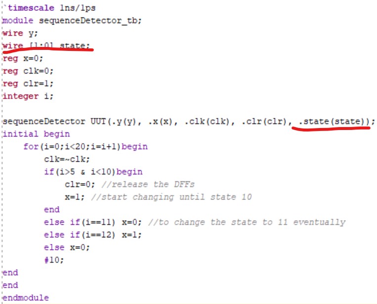
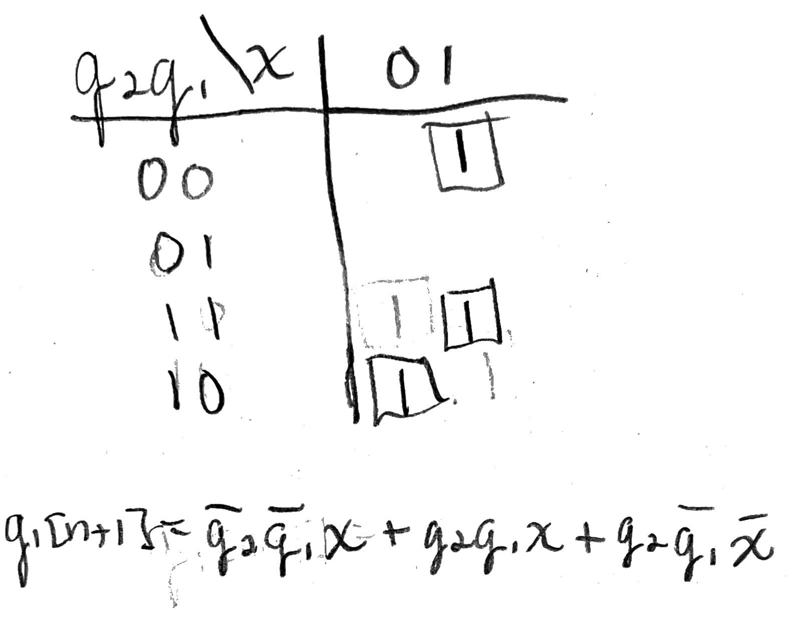
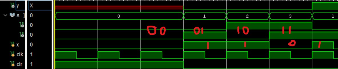
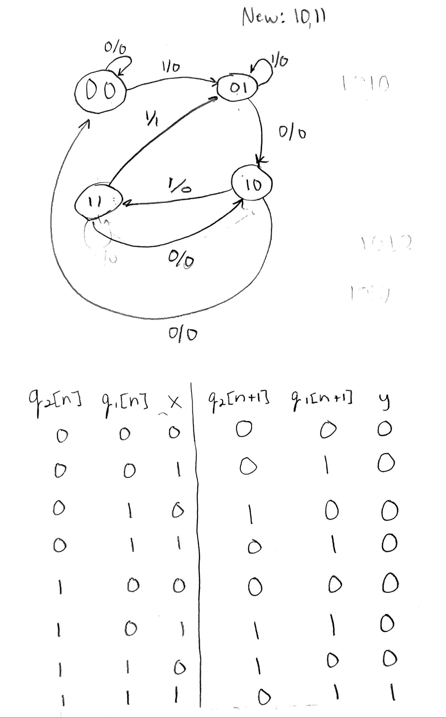
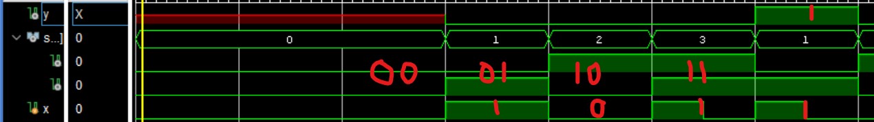
For the new squence 1011
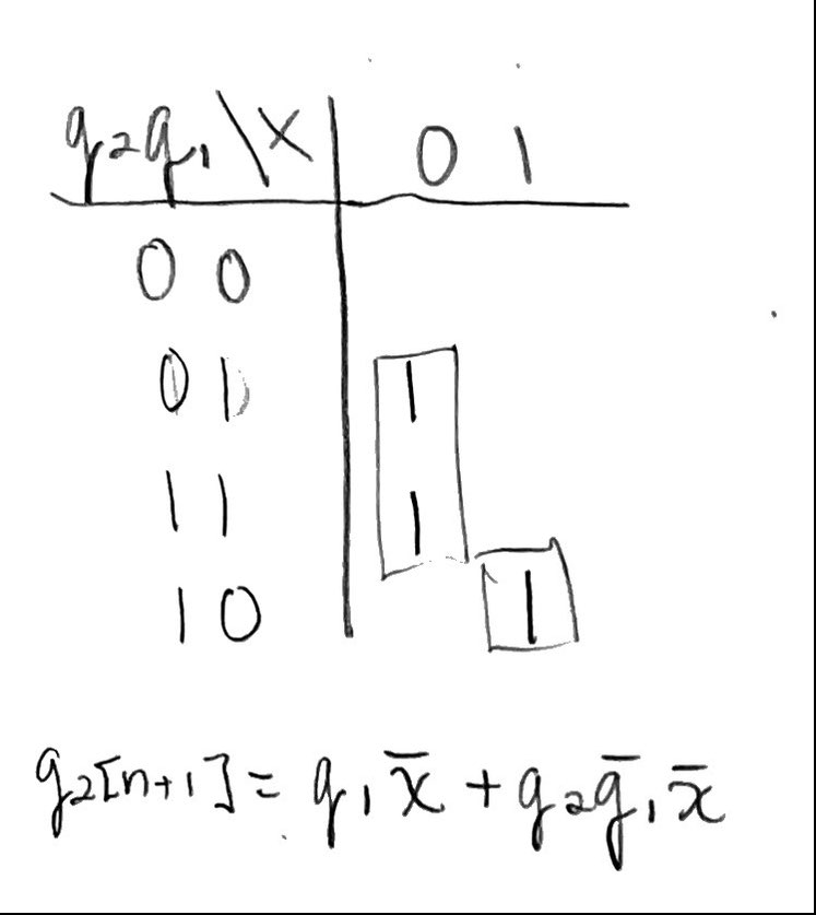
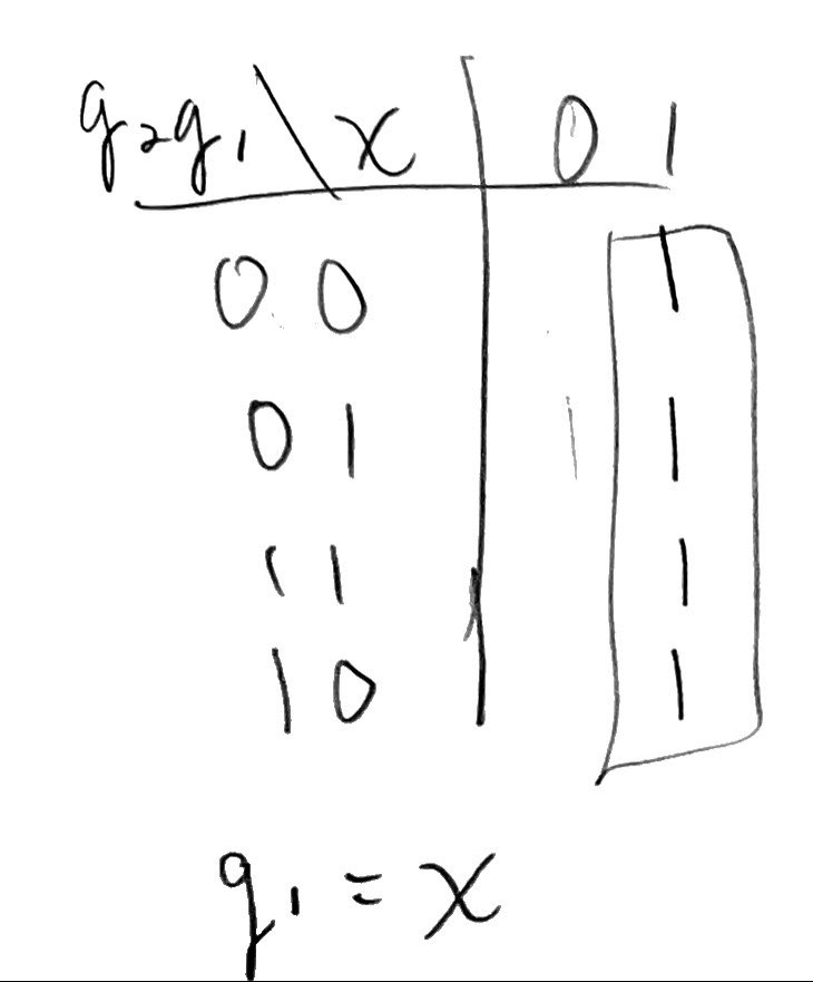
Note that q1 should be q1[n+1] for the equation and y again is y=q2[n]q1[n]x.
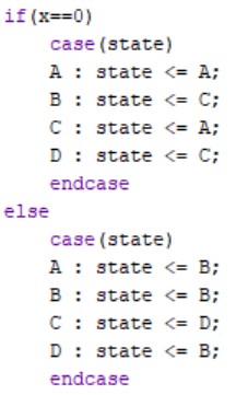
Task 3 - Similar to the sequence detector in Section 3, change the sequence to be detected to 1011, design the state diagram, draw the truth table, find the logic equations, and design the verilog module and testbench to verify the logic.
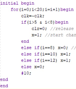
The verilog code only needed to be changed a little from the original sequence. The two images above show where the changes were made.
Task 4 - Simulate the four types of shift registers in Section 5.
Task 2 - Repeat the work in Section 3. Use two methods, the given one and the behavioral one. Show simulation results.
Given method.
Behavoioral method
For the new squence 1011
Note that q1 should be q1[n+1] for the equation and y again is y=q2[n]q1[n]x.
Task 3 - Similar to the sequence detector in Section 3, change the sequence to be detected to 1011, design the state diagram, draw the truth table, find the logic equations, and design the verilog module and testbench to verify the logic.
The verilog code only needed to be changed a little from the original sequence. The two images above show where the changes were made.
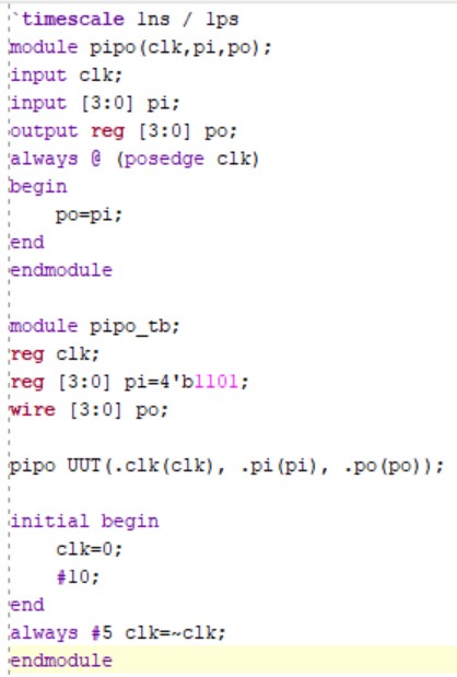
Task 4 - Simulate the four types of shift registers in Section 5.
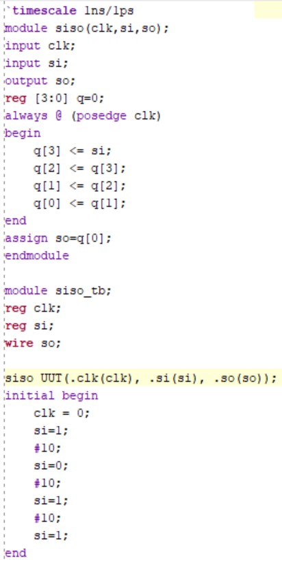
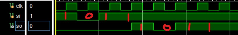
Serial In Serial Out
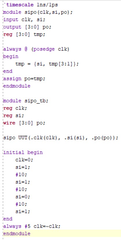
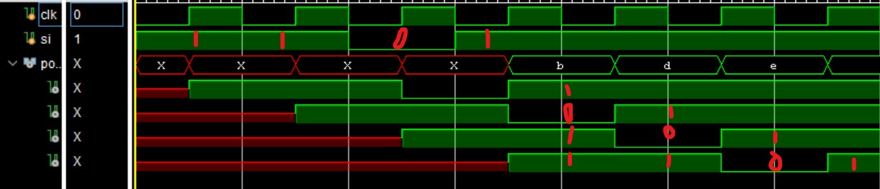
Serial In Parallel Out
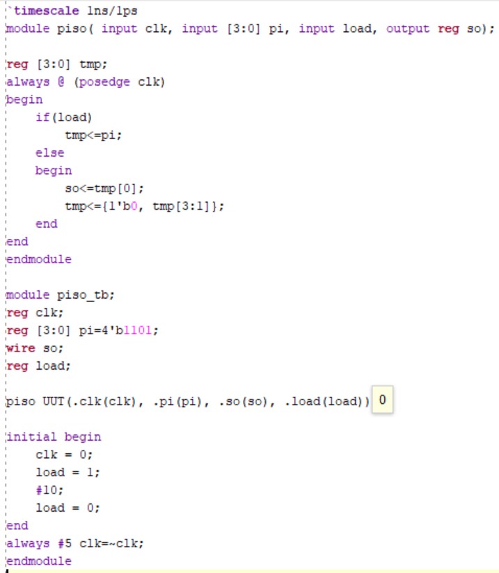
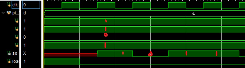
Parallel In Serial Out
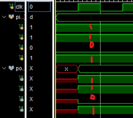
Parllel In Parallel Out
Task 5 - Build a counter module and show the simulation results.
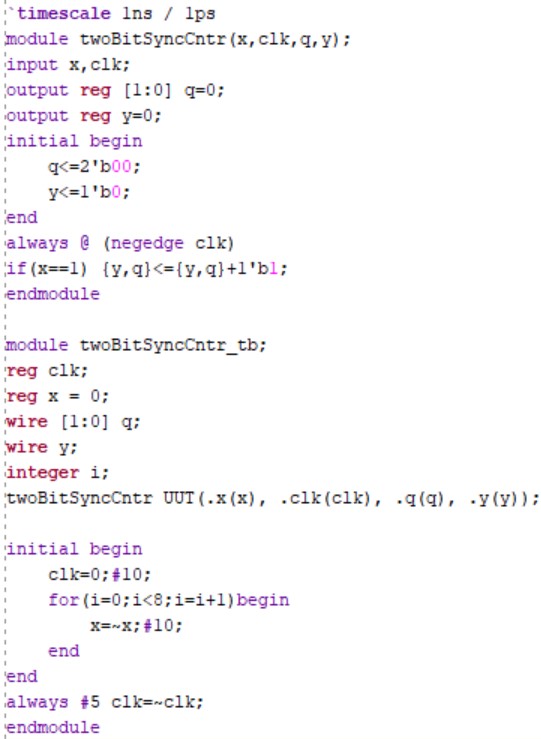
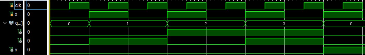
This was verified using the truth table.
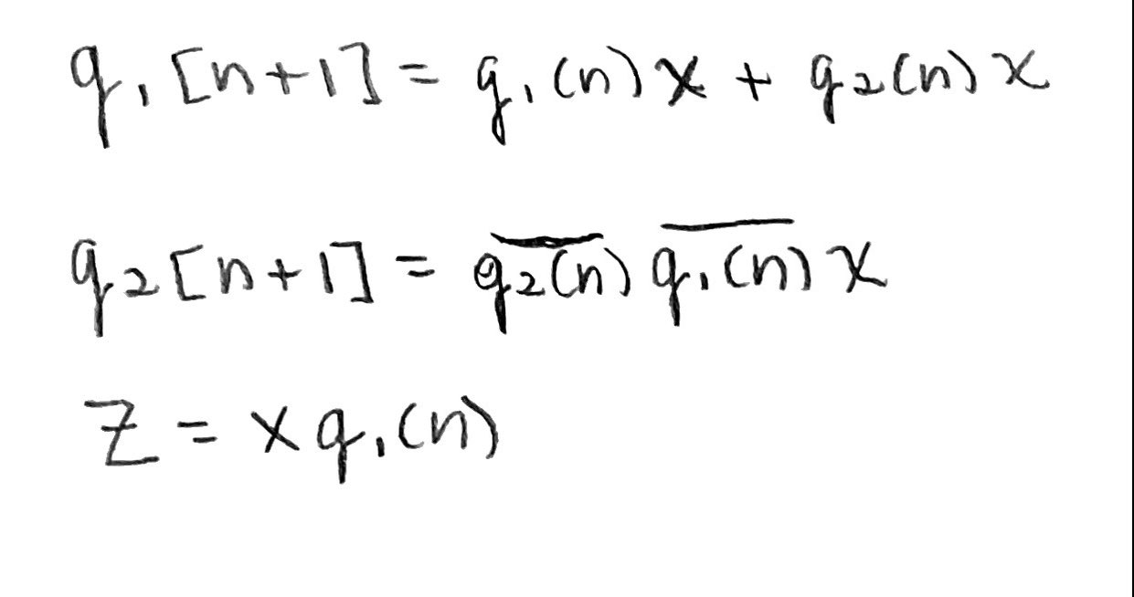
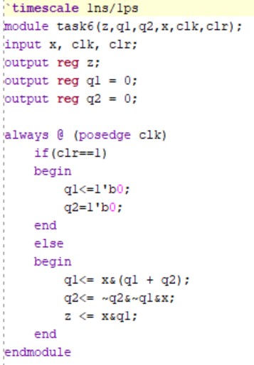
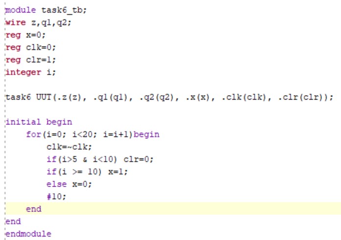
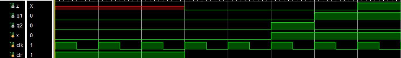
Task 6 - Find the logic equation of the following circuit and implement it in verilog. Show the simulation results.
Serial In Parallel Out
Parallel In Serial Out
Parllel In Parallel Out
Task 5 - Build a counter module and show the simulation results.
This was verified using the truth table.
Task 6 - Find the logic equation of the following circuit and implement it in verilog. Show the simulation results.