CE433 Embedded Devices
HW2
- Combinational Logic Blocks

Connor O'Keefe
Email: cwokeefe@fortlewis.edu

Task 1: Simulation of half adder and full adder
The half-adder (a) and the full adder (b) are shown below.


(a)


(b)


Task 2: Design of a testbench for the one-bit comparator


Task 3: Design of a testbench for the 4-bit comparator


Task 4: Implimenting a 2-bit comparator on the Basys 3 board


Task 5: Design of the testbench for the 2-to-4 decoder


Task 6: Find Q2 and Q1 for the 8x3 priority encoder, build the module and verify

Q2 = D4 + D5 + D6 + D7
Q1 = ~D5~D4(D2+D3) + D6 + D7

Scratch work is show below.


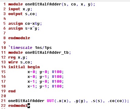
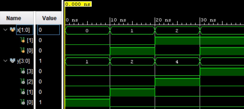
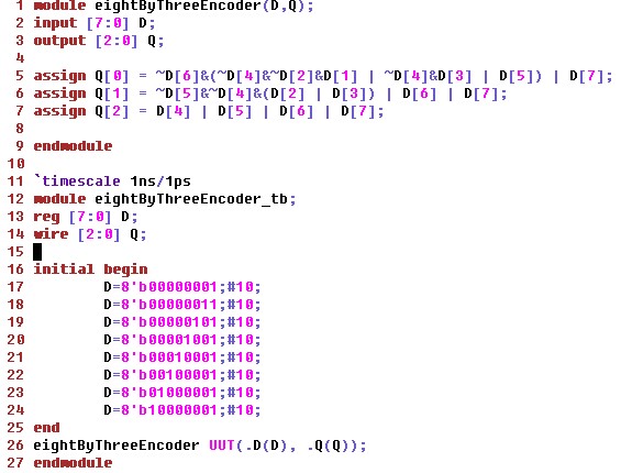
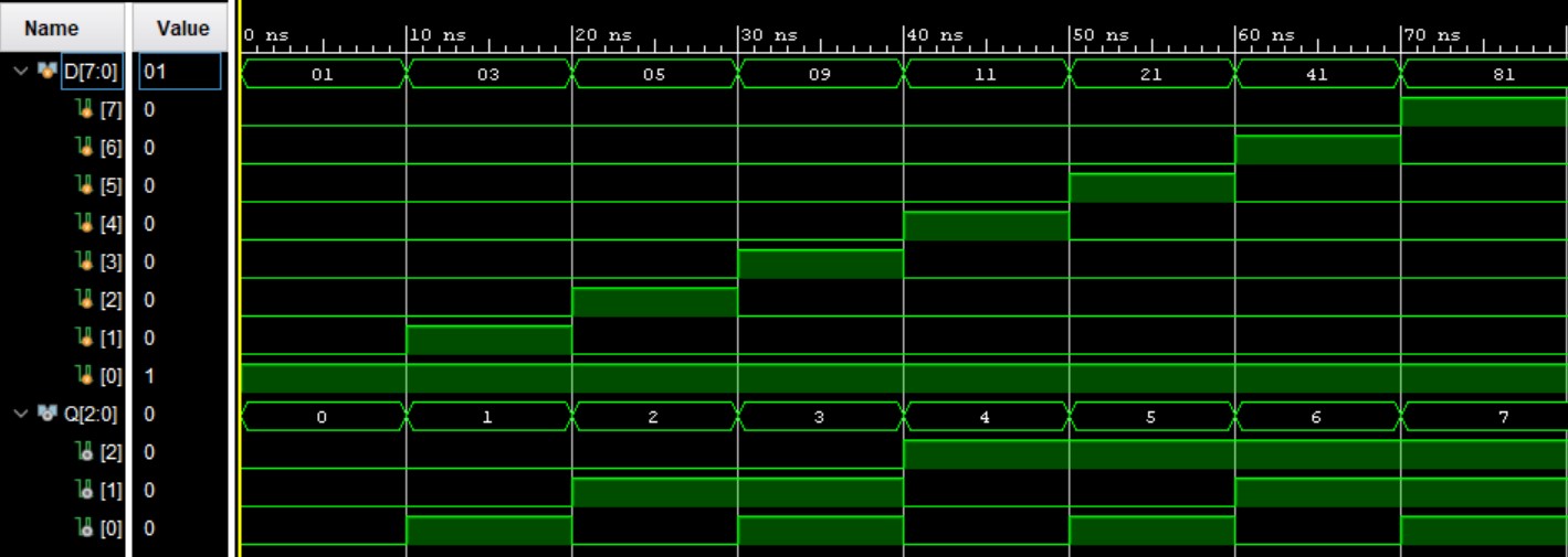
Then we may make the module and simulate to verify.


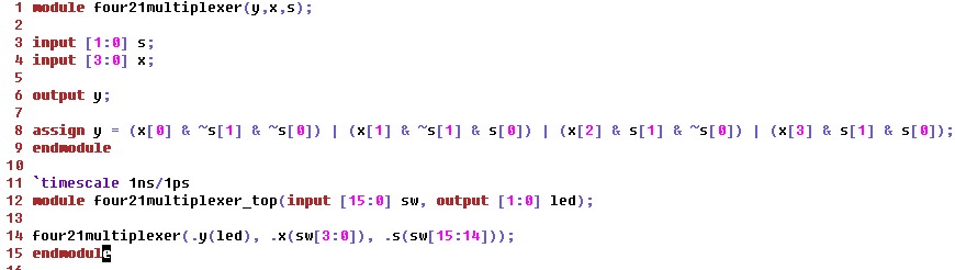
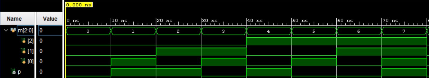
Task 7: Implement a 4-1 multilplexer on the Basys 3 board.


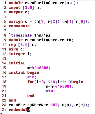
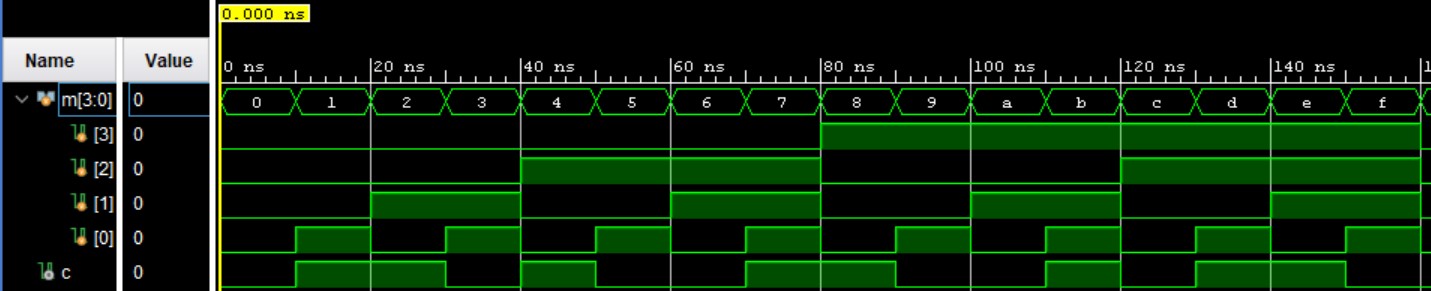
Task 8: Design/Verify an even parity generator and checker in simulation. Impliment an even parity checker on the Basys 3 board.
The even parity generator (a) and checker (b) are shown simulated below.


(a)


(b)
Here is a video of a even parity checker.


Task 9: Impliment the home alarm system and the garage parking counter of the Basys 3