CE433 Embedded Devices
Lab 5
- 2's Complement Adder

Connor O'Keefe
Email: cwokeefe@fortlewis.edu

Introduction
This lab is to design a 2's complement adder which will add and subtract using input from the switches and output onto the SSD.

Materials and Methods
  1. Basys 3 FPGA
  2. Vivado
  3. gVim

Procedure

Previously, full adders were already implimented and may be used for the module with changes to the top module for communication with the board. In Figure 2, the top module for the 2's compliment is shown. Figure 2 shows all of the code that was implementedfor the lab.


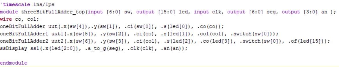
Figure 1. Top module for the 3-bit full adder, being the 2's compliment top.
   
       
                                                                                                                          (a)                                                                                       (b)                                                                     (c)
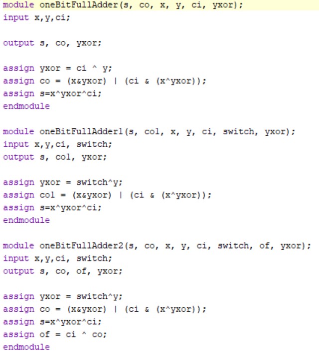
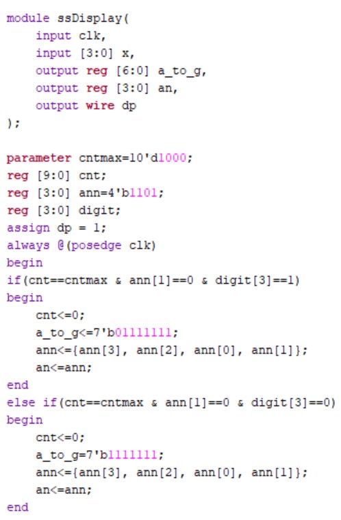
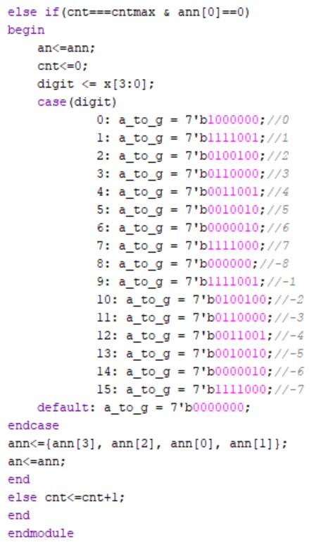
Figure 2. The 3-bit full adder module (a) and the seven segment display module (b).


Results
The 2's complement full adder was successfully implimented onto the FPGA shown in the video below. Note that the first switch, sw0, "activates" 2's complement. The next three switches, being sw3, sw2, and sw1, are the next three bits which will be added or subtracted from the next three switches; sw6, sw5, and sw4.  Where switches sw3 and sw6 are the MSB bits and switches sw1 and sw4 are the LSB bits.


Unfortunately, I was unable to generate a negative sign with subratction.

Discussion
This lab did present some troubles, but overall when the task was completed it showd how much work goes into what seems to be simple. In time I will hopefully generate the negative sign on the SSD.