ENGR-433 Spring 2023
Lab 4: Combinational Logic Blocks
Name: Cheyenne Tucson
Email: crtucson@fortlewis.edu

Combinational Logic Blocks on a FPGA

1. Introduction

Proficiency with combinational logic is crucial for an ASIC engineer. Through this lab, a traffic light controller and an even-parity checker/generator system were described in Verilog, simulated in Vivado, and implemented on a FPGA via a Basys3 protoboard.


2. Materials


3. Procedure

Vivado was opened on a PC; a new RTL project was created, the appropriate chipset was selected for compatability with the Basys 3 board, a .xcf constraint file was attached to the project.

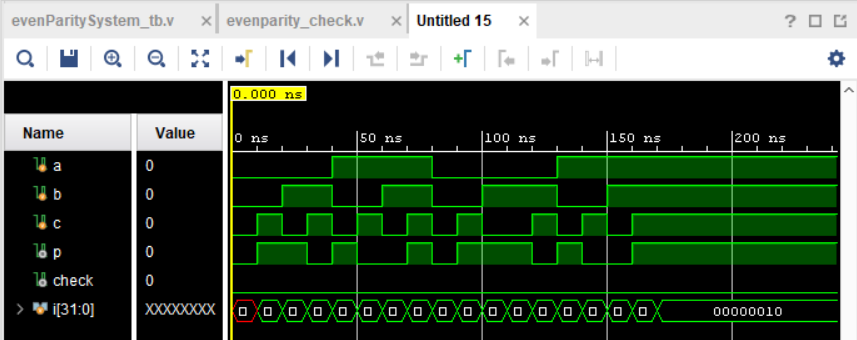
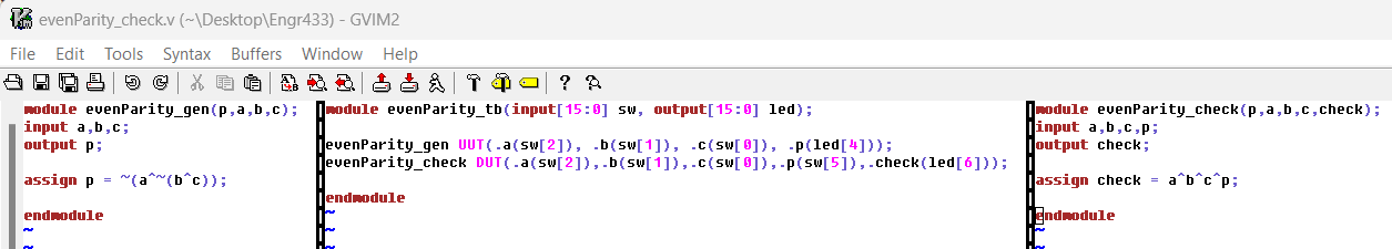
Verilog scripts for the following combinational logic blocks were written in gVim: a traffic light controller, and an even-parity generator/checker. 
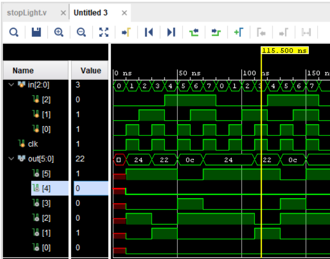
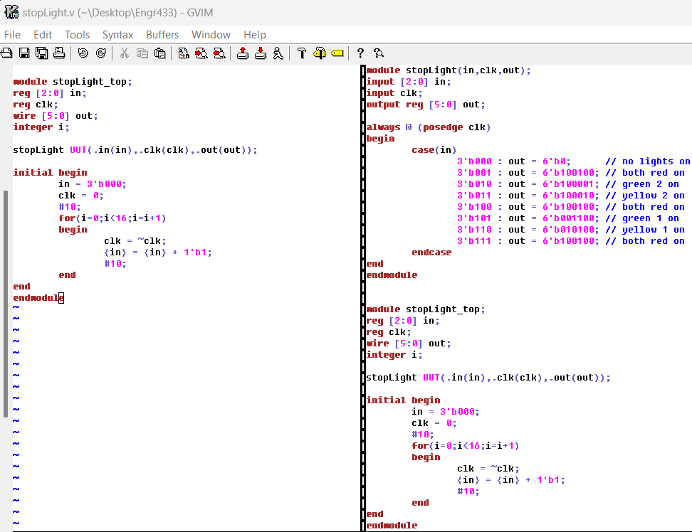
The digital circuit for the traffic light controller was described in gVim with Verilog HDL. Testbench scripts were then written in Verilog for both behavioral simulation and FPGA implementation for each combinational logic block. Once these scripts were completed, they were added to the project in Vivado and simulated/synthesized and the Basys 3 board was programmed with the bitstream files generated for each digital circuit described.


4. Results

The behavioral simulation results of the traffic light controller can be found in Figure 1 below, and the Verilog scripts used to describe the circuit can be found in Figure 2.
The recorded demonstration of the traffic light controller implemented on the FPGA can be found in Video 1 below.

Figure 1. A screen-snip of the behavioral simulation ran of the traffic light controller.                                                      Figure 2. A screen-snip of the Verilog scripts used to describe the digital circuit of the traffic light controller.

Video 1. A recorded demonstration of the traffic light controller implemented on the FPGA. The first LED on the left represents the red light of the first traffic signal, the LED to the right of the leftmost LED represents the yellow light of the first traffic signal, and the LED on the right of that LED represents the green light of the first traffic signal. The rightmost LED represents the green light on the second traffic signal, the LED to the left of that represents the yellow light on the second traffic signal, and the LED to the left of that represents the red light on the second traffic signal.


The behavioral simulation results of the even-parity generator/checker system can be found in Figure 3 below, and the testbench script can be found in Figure 4. The recorded demonstration of the even-parity generator/checker can be found in Video 2 below.
               
Figure 3. A screen-snip of the behavioral simulation of the even-parity generator/checker.                                                              Figure 4. A screen-snip of the Verilog testbench written to implement the even-parity generator/checker on the FPGA.

Video 2. The recorded demonstration of even-parity generator/checker being implemented on the FPGA. The leftmost LED indicates whether the value passes the even-parity check (with the LED on meaning it fails.) The rightmost LED indicates if a parity bit was generated (with the LED on to indicates the bit was generated.) The generated parity bit is input to the checker via the leftmost switch being used on the Basys3 board to show the functionality of the circuit is correct.


5. Discussion

Being able to implement combinational logic blocks within digital circuits is not as intimidating as it seems. The skills polished through completing this lab will surely help me in the future as an ASIC Engineer in the industry.