Task 1
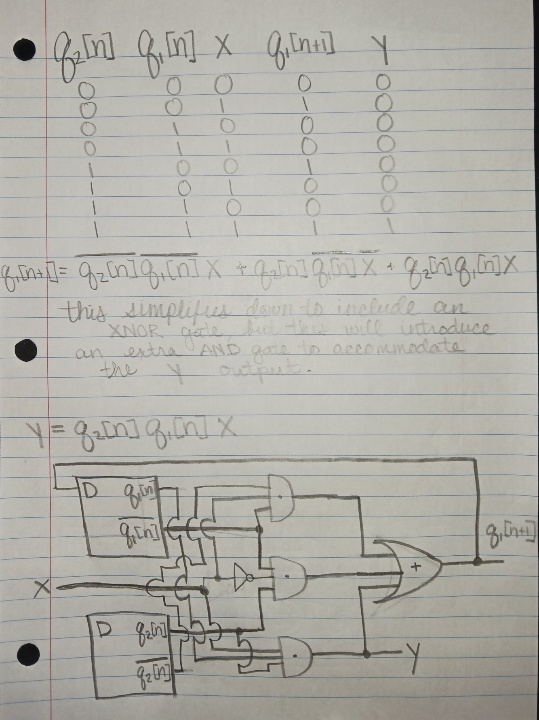
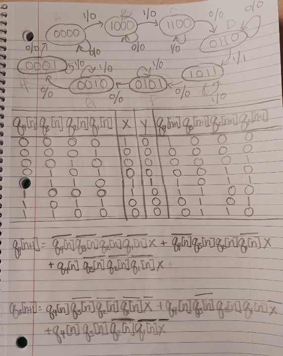
For the first task, the logic equation for q_1[n+1] and y were found by looking at the
State Table for the circuit. The gate-level schematic was created from the logic equation;
this can be found in Figure 1 below.
For the first task, the logic equation for q_1[n+1] and y were found by looking at the
State Table for the circuit. The gate-level schematic was created from the logic equation;
this can be found in Figure 1 below.
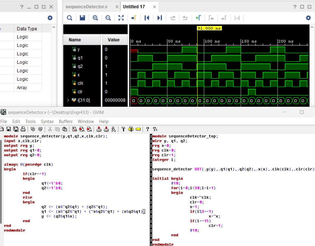
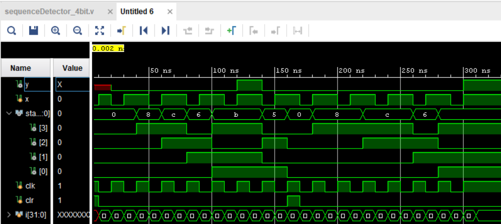
After the logic equation and schematic was found and drawn, a sequence detector circuit was described
in Verilog by looking at both the logic equation found in Task 1, and the Meeley State Diagram of the
State Table from Task 1. Behavioral simulations were ran for each version of the sequence detector circuit.
These can be found below in Figures 2a and 2b.
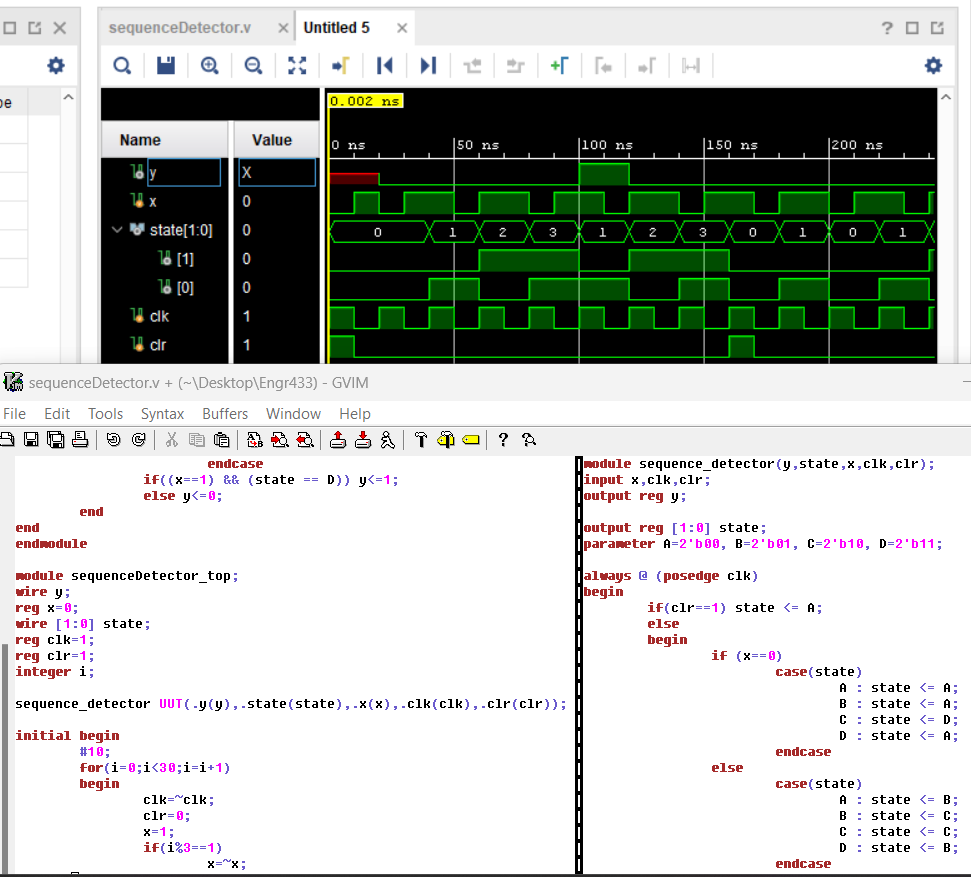
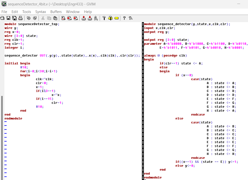
Once the sequence detector was simulated in Task 2, a Meeley State Diagram was constructed
to detect the sequence to 1011. The truth table of the state diagram was drawn out, and the logic
equations were found from the truth table. Once the logic equations were found, a sequence detector
circuit was described in Verilog to confirm the sequence is detected properly. These can be found in
below in Figures 3a, 3b, and 3c.
 f3c;
f3c;
After the sequence detectors were completed and functioning as expected, four different types of
shift registers were described in Verilog and simulated in Vivado. The types of shift registers
described and simulated are as follows: Serial-In-Serial-Out (SISO), Serial-In-Parallel-Out (SIPO),
Parallel-In-Parallel-Out (PIPO), and Parallel-In-Serial-Out (PISO). Screen-snips of the Verilog scripts
behavioral simulations of each type of shift register can be seen below, respective to the list above,
in Figures 4a-4x, 5a-5x, 6a-6x,and 7a-7x.
A counter module was described and simulated with Vivado and Verilog. The screen-snips of the behavioral simulation and Verilog scripts can be found below in Figure 8.
A gate-level schematic was provided for us. From this schematic, the logic equation
of the circuit was found. Once this was found and simplified to my liking (as allowable through
Boolean algebra,) the digital circuit was described in Verilog and a behavioral simulation was
ran in Vivado. The logic expression can be found below in Figure 9a, and the simulation and
Verilog scripts can be found in Figure 9b and 9c.