ENGR433 Spring 2023
Homework 4
Name: Cheyenne Tucson
Email: crtucson@fortlewis.edu

Data Storage

Task 1

For the first task, a level-triggered SR Latch/Flip-flop was described in Verilog and simulated in Vivado. The script and results of the simulation for the SR Latch can be found in Figure 1 below. The SR Flip-flop script and simulation results can be found in Figure 2 below.

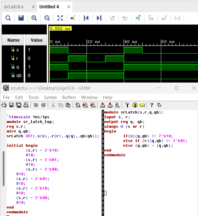
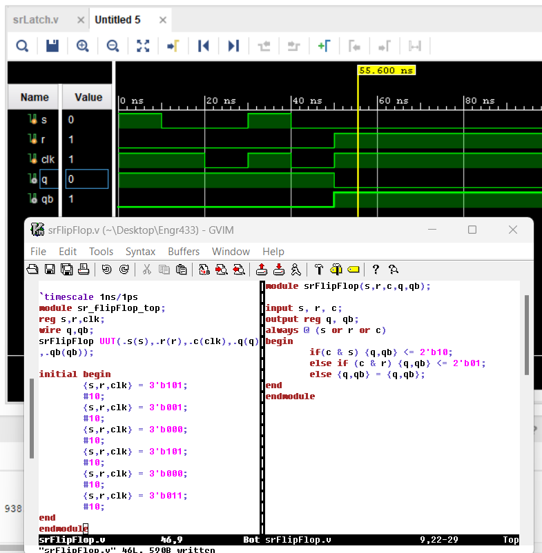
Figure 1. This is a screen-snip that contains the script and simulation results for the SR Latch.                          Figure 2. This is a screen-snip that contains the script and simulation results for the SR Flip-flop.


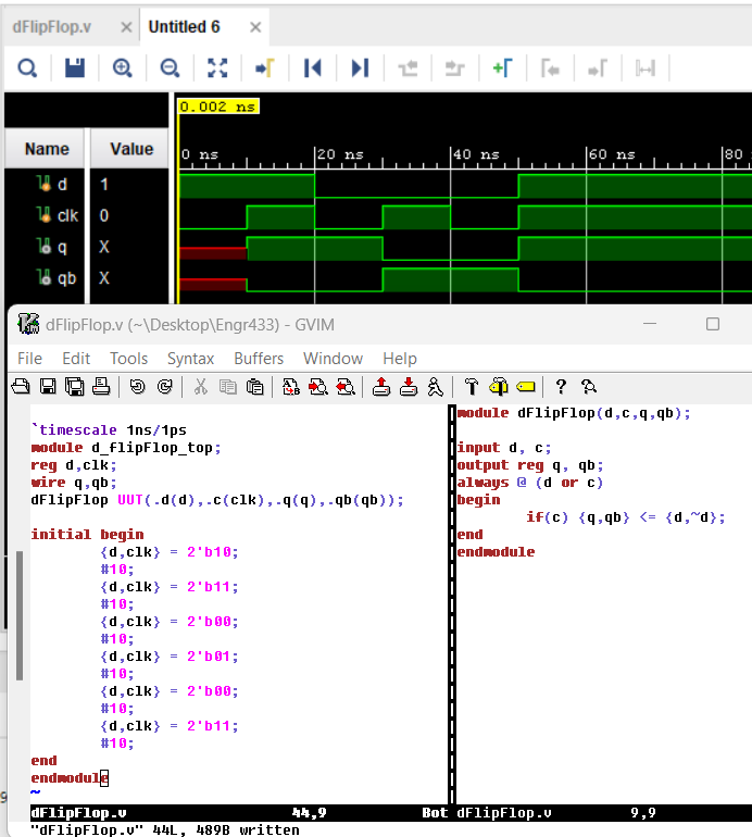
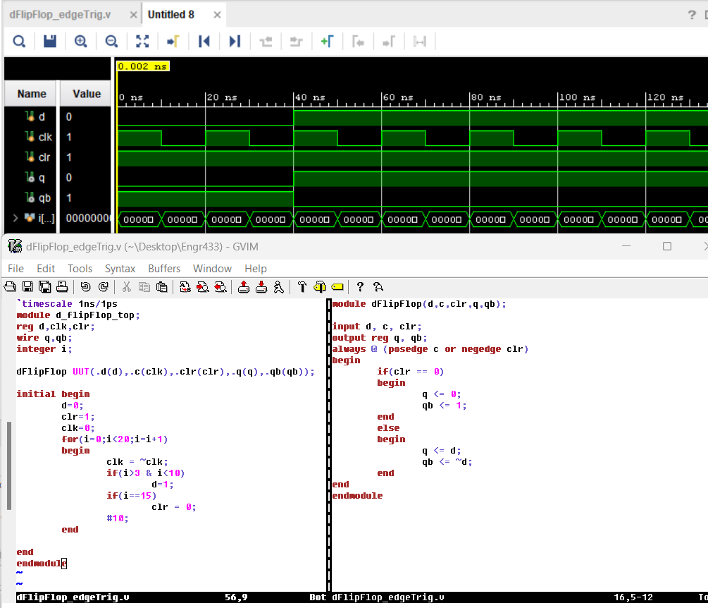
After the SR Latch and Flip-flop were done, a Data Flip-flop (D Flip-flop) was described in Verilog and simulated in Vivado. Both the level-triggered and edge-triggered versions were described in Verilog and simulated in Vivado. The results for the Level-triggered D Flip-flop can be seen in Figure 3 below. The Edge-triggered verision of the D Flip-flop can be seen in Figure 4 below.

              
Figure 3. This is a screen-snip of the simulation results and Verilog script used to describe a Level-triggered Data Flip-flop.                Figure 4. This is a screen-snip of the simulation results and Verilog script used to describe an Edge-triggered Data Flip-flop.


Task 2

After the D Flip-flops were completed, the JK Flip-flop was described and simulated. These results can be found in Figures 5a and 5b below. After the JK Flip-flop was finished, it was turned into a Toggle Flip-flop. The scripts and simulation results can be found in Figure 6 below.


Figure 5. This is a screen-snip that contains the script used for the behavioral simulation of the JK Flip-flop.                  Figure 5b. This is a screen-snip of the behavioral simulation results from Vivado of the JK Flip-flop.


Figure 6. This is a screen-snip that contains both the simulation results and Verilog script used to describe the T Flip-flop.

Task 3

For the final task, a Read-Only Memory (ROM) digital circuit was described in Verilog. various versions of the ROM were described: an 8-bit binary reader with a byte of storage capacity, a 3-bit binary reader with 4-bits of storage capacity, an 8-bit hexadecimal reader with 4-bits of storage, and a 16-bit hexadecimal reader with a 2-bit memory depth. Examples of these can be found below in Figures 7 through A.

Figure 7a. A screen-snip of the simulation results of the 8-bit binary ROM.                                                                         Figure 7b. A screen-snip of the Verilog script used to describe the 8-bit binary ROM.


Figure 8. A screen-snip of the 16-bit hexadecimal ROM simulation and necessary Verilog scripts.


Figure 9. A screen-snip of the 8-bit hexadecimal ROM simulation and necessary Verilog scripts.


Figure A. A screen-snip of the 3-bit binary ROM simulation and necessary Verilog scripts.

Another ROM was generated with Vivado via an IP core. A file called "dsImage.coe" is defined as the memory file to be read with this ROM. This was documented below in Figures B1-B3.

                                                                                    
Figure B1. This is a screen-snip of the ROM that was generated in Vivado via an IP core.                 Figure B2. This is a screen-snip of the testbench script written in Verilog used for the behavioral simulation.                
Figure B3. This is a screen-snip of the simulation results of the ROM reading the "dsImage.coe" file.