ENGR433 Spring 2023
Homework 1
Name: Cheyenne Tucson
Email: crtucson@fortlewis.edu
Homework 1
Task 1
Using gvim and Vivado software, behavioral simulations of a simple logic circuit were conducted using three different methods in a hardware description language (HDL). Verilog is the HDL used to describe these digital circuits.
The first method used was Structural Modeling. The code and simulation for the structural modeling method can be found in PDF 1, Figure 1. The second method used was the Dataflow Modeling method. The code and simulation can be found in PDF 1, Figure 2.
PDF 1. This is a PDF that contains all the screen-snips of the simulation results in Vivado and Verilog code in gvim. Page 1 contains Figure 1 and the results of the Structural Modeling; page 2 contains Figure 2 and the results of the Dataflow Modeling simulation; page 3 contains Figure 3 and the results of the Behavioral Modeling simulation.
The final method used was the Behavioral Modeling method. This method utilized a sensitivity list to trigger the defined behavior(s) within the always block, a type of proceedural block.
Task 2
Verilog features both Blocking and Non-blocking behavior. Blocking assignments block execution of the next statement until the line assigned the blocking behavior is completed. These are best used in combinational circuits. The non-blocking assignment will execute in parallel with all other non-blocked lines; these are best used in sequential circuits.
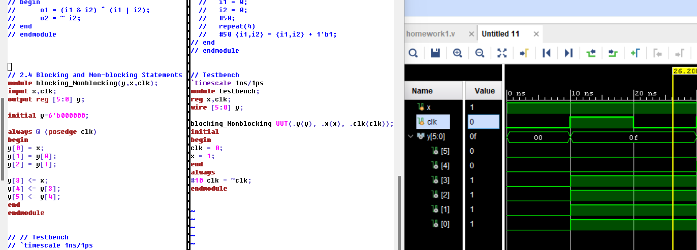
Figure 4. A screen-snip of the behavior simulation ran in Vivado; also included is the Verilog code of the blocking and non-blocking behavior along with the testbench code.
Task 3
An important aspect in designing digital circuits is timing. Timing can be controlled with a clock, and delays can be implemeted into the circuit to help affect the functionality to achieve specific goals with the circuit.
First, A 20 ns delay was described for the second output in this circuit simulation. The results are shown on the left side of Figure 5 below.
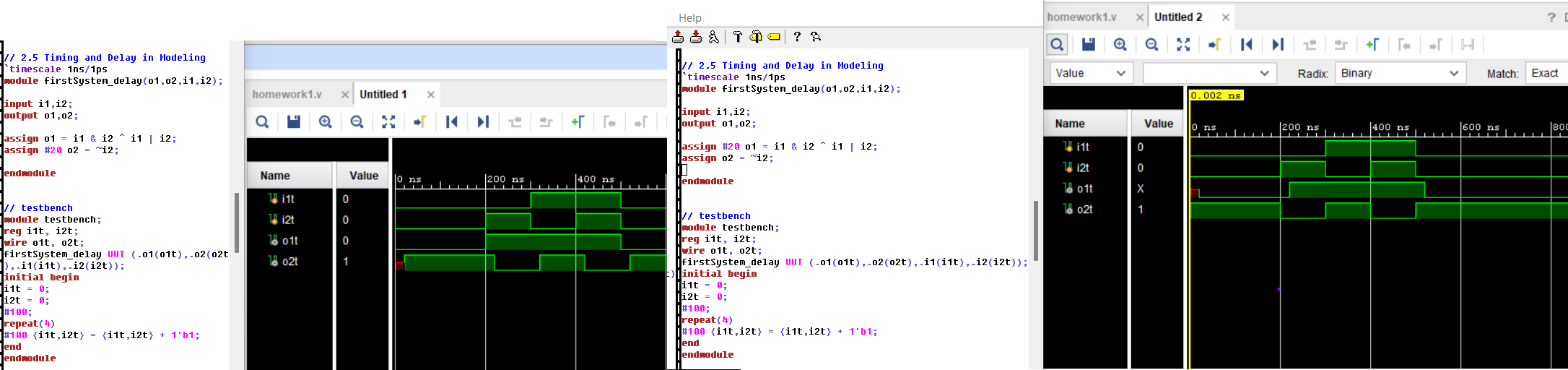
Figure 5. A screen-snip of the behavior simulation ran in Vivado; on the left is the simulation with Verilog module and testbench code with the delay on output 2 (o2), and on the right is the simulation and Verilog code for the delay implemented on the first output (o1).
Task 4
For the next task, the delay was moved from the second output to the first output to demonstrate the difference in the output. After this delay was implemented on the second output, the delay was moved to the first output. The difference can be seen in the right side of Figure 5 above.
A hand draw timing diagram of the output of the digital circuit can be seen in Figure 6 below.
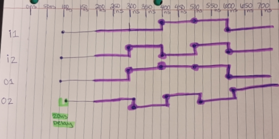
Figure 6. A hand-drawn timing diagram of the digital circuit described in Verilog with the 20 ns delay on the second output.
Task 5
Sometimes a digital circuit needs a hierarchy implemented in the functionality of the design. With Verilog, multiple modules can be written in the same '.v' file so long as the modules have different names. However, this can also be implemented through separate '.v' files added to the design sources individually before running a behavioral simulation in Vivado.
An example of this can be seen in PDF 2 below.
PDF 2. This PDF contains the screen-snips of the Verilog code in gvim, the Design Sources list contained in the project, and the behavioral simulation from Vivado in that respective order.