1. Introduction
Knowing how a Succesive Approximation Register (SAR) operates is crucial to understanding how a SAR ADC converts a voltage sampled at a moment into a digital translation. The SAR is constructed of many D Flip-flops that have set/reset functionality. The D Flip-flop specifically used in this SAR is based off a circuit from Texas Instuments (TI) that is intended for commercial use; This flip-flop is made of 3-input NAND gates. For this assignment, a 3-input NAND gate will be constructed in LTSpice out of NMOS and PMOS transistors and have a symbol created for use in other schematics. The D-Flip-flop will be built out of NAND gates, and the flip-flop will be used to build the 8-bit SAR block. Each will be simulated in LTSpice to confirm functionality before using it to build the other circuits.
3. Procedure
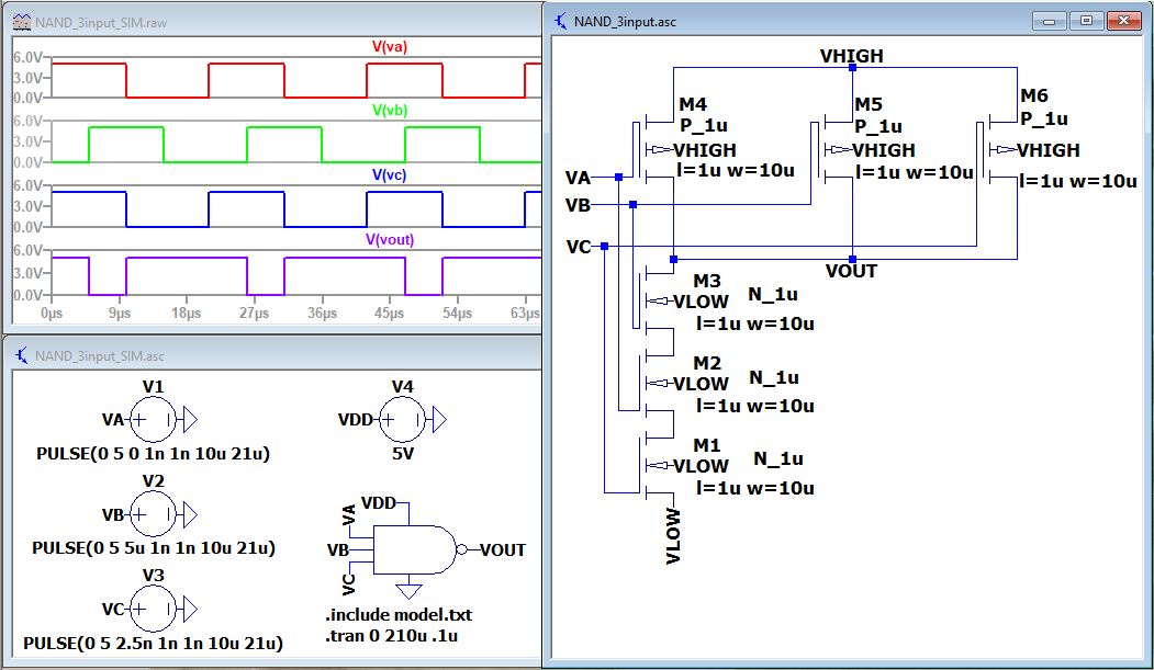
First, the schematic for the 3-input NAND gate was created. I had one made from a previous class I took, but I decided to recreate it for extra practice. This can be seen in Figure 1 below. After the schematic was finished, I created a symbol from the schematic to make using this NAND gate in other schematics easier. This also can be seen in Figure 1. Once the symbol was finished, I created a new schematic to simulate the NAND gate and verify that it works as intended.
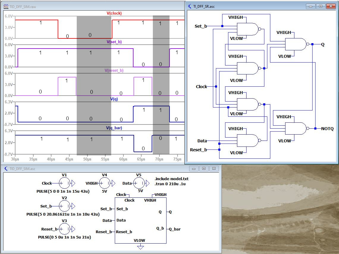
Once the functionality was confirmed, I used the NAND gate I just made to create a new schematic of the D-Flip-flop. I created a symbol for the D-Flip-flop, and then created a schematic to simulate it. These all can be seen below in Figure 2.
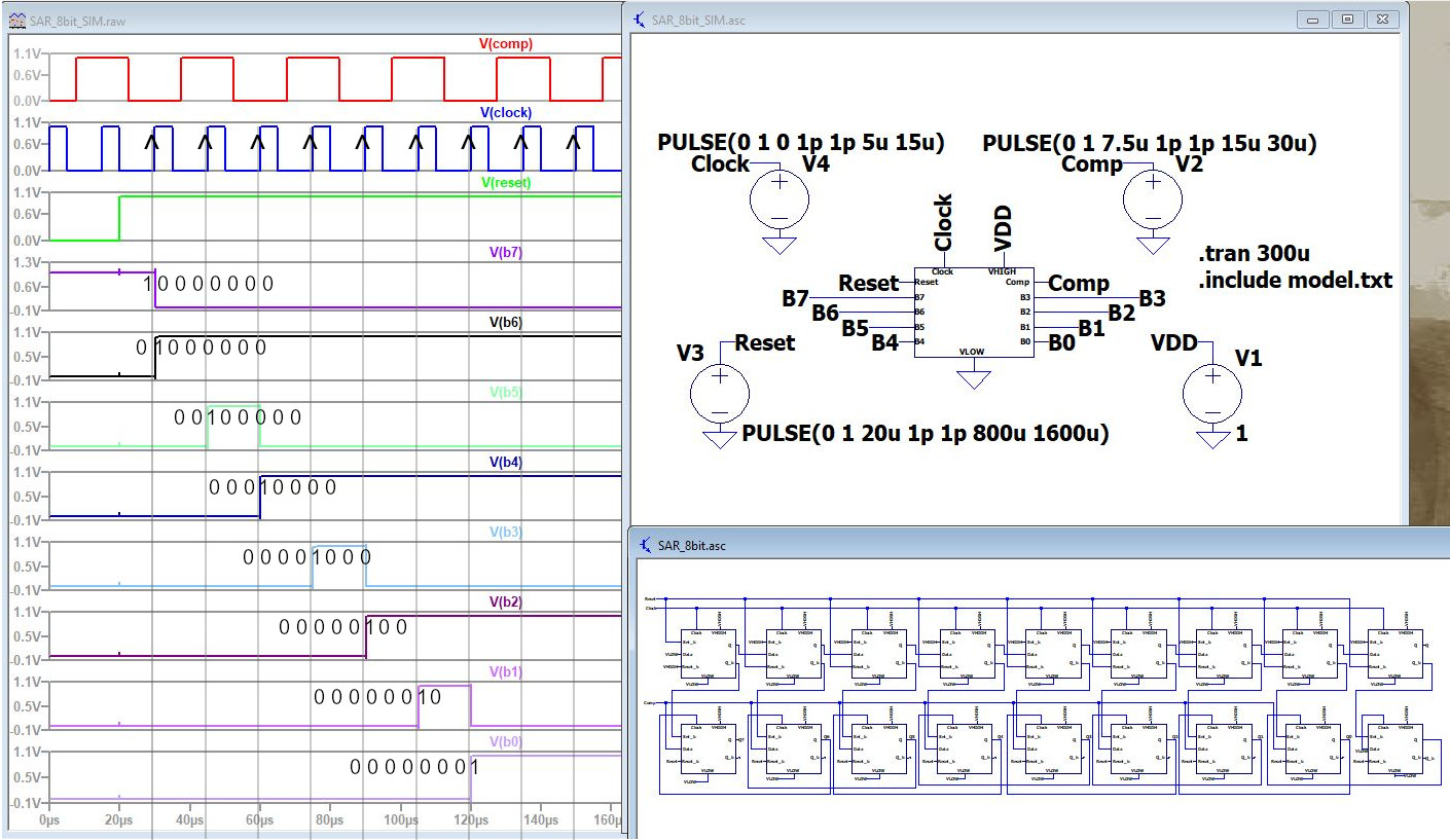
Once the D-Flip-flop was verified, I created a 8-bit SAR out of the D-Flip-flops that were just made. I made the symbol and simulation schematic to ensure it works as planned. These can all be found in Figure 3.
5. Discussion
I did notice that the output of the NAND gate was wonky when I built it with the 50n NMOS and PMOS transistors. The output would slowly creep back to the full scale voltage and never reach 0V. To correct this issue, I reduced the size of the tranistor to 1u x 10u like the one I built while taking Fundamentals of Logic back in the Summer of 2020. This corrected the output to as I expected. I also noticed that the impossible cases of input combinations in the D-Flip-flop from TI came out to be valid in the simualtion. I think this is either because LTSpice gives an ideal simulation or because I could not get the correct simulation outputs with the 50n versions of the NMOS and PMOS transistors from the model.txt file. I will look into this further to make sure that this issues was not caused by an error in my schematic design.