1. Introduction
The inverter is a crucial circuit to know as a computer engineer. It can be used in various instances to customize a product to accomplish a specific task. Usually this is needed when there are conditional cases.
In this lab, we will create an inverter using CMOS transistors, scale it by multiplying the lengths to create a larger inverter, and simulate the results in both LTSpice and two of the built-in simulators that Electric VLSI has to offer.
3. Procedure
To begin, I opened Electric VLSI and copied the NMOS and PMOS schematics from the last lab onto a new schematic cell. The schematic cell was named "Inverter{sch}." I then changed the PMOS width to 20, and made the connections as seen in Figure 1. I also created the icon view and changed the icon to look like a NOT gate logic symbol. Once that was in order, I ran a DRC to ensure there were no errors in the schematic.
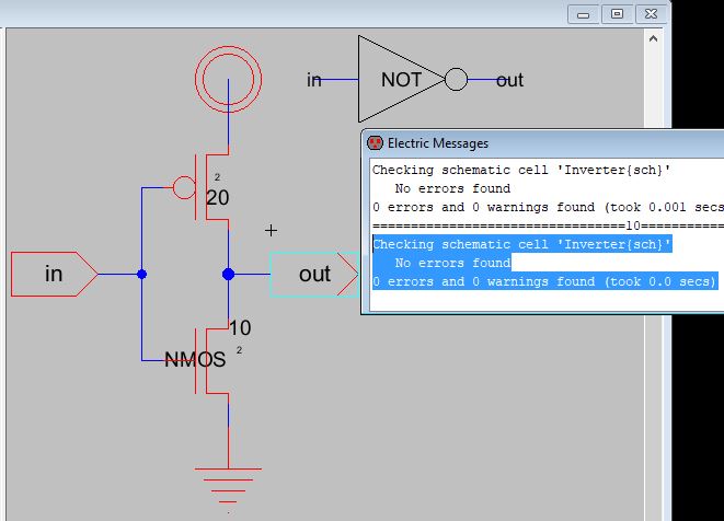
Figure 1. This is a screen-snip of the Inverter{sch} schematic in Electric VLSI. The icon is shown in the blue box in the upper right corner, and the DRC results are shown in the text box, highlighted in blue. No errors were reported.
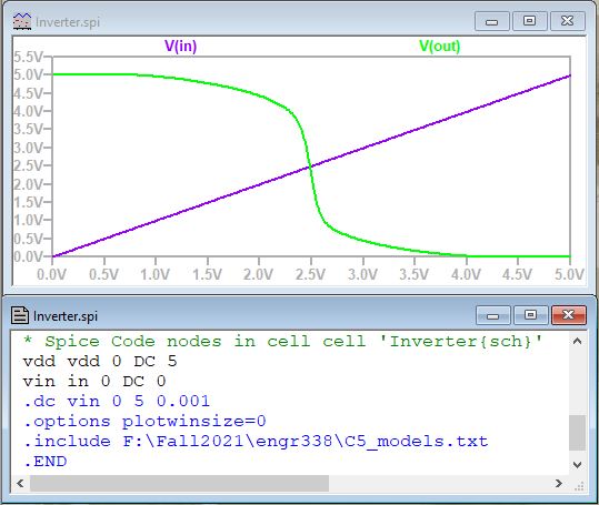
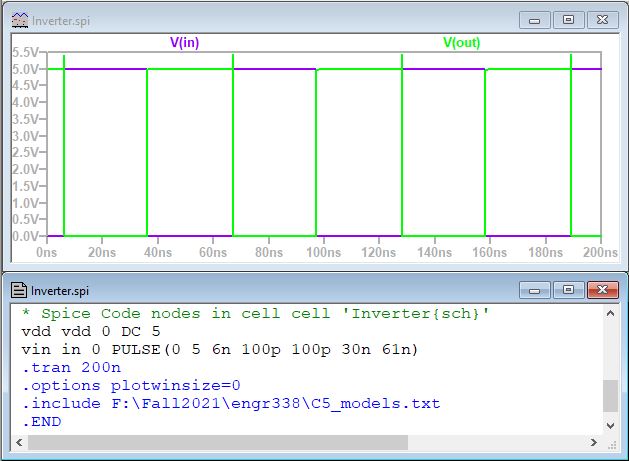
I ran a simulation that plotted the voltages of V(in) vs. V(out). The SPICE code and results of this simulation are seen in Figure 4. After, I ran another simulation of a transient analysis with V(in) set to pulse between 0 and 5 volts. The simulation results and SPICE code can be seen in Figure 5.
Next I created the layout of the inverter. I did so by putting a PMOS, NMOS, two nActs and pActs each, an nWell and a pWell, a metal-1 to poly-1 and a metal 1 pin on the layout and making the proper connections as show in the external tutorial linked in the lab instructions. This can be seen in Figure 2 along with the DRC, LVS, and well checks for the layout.
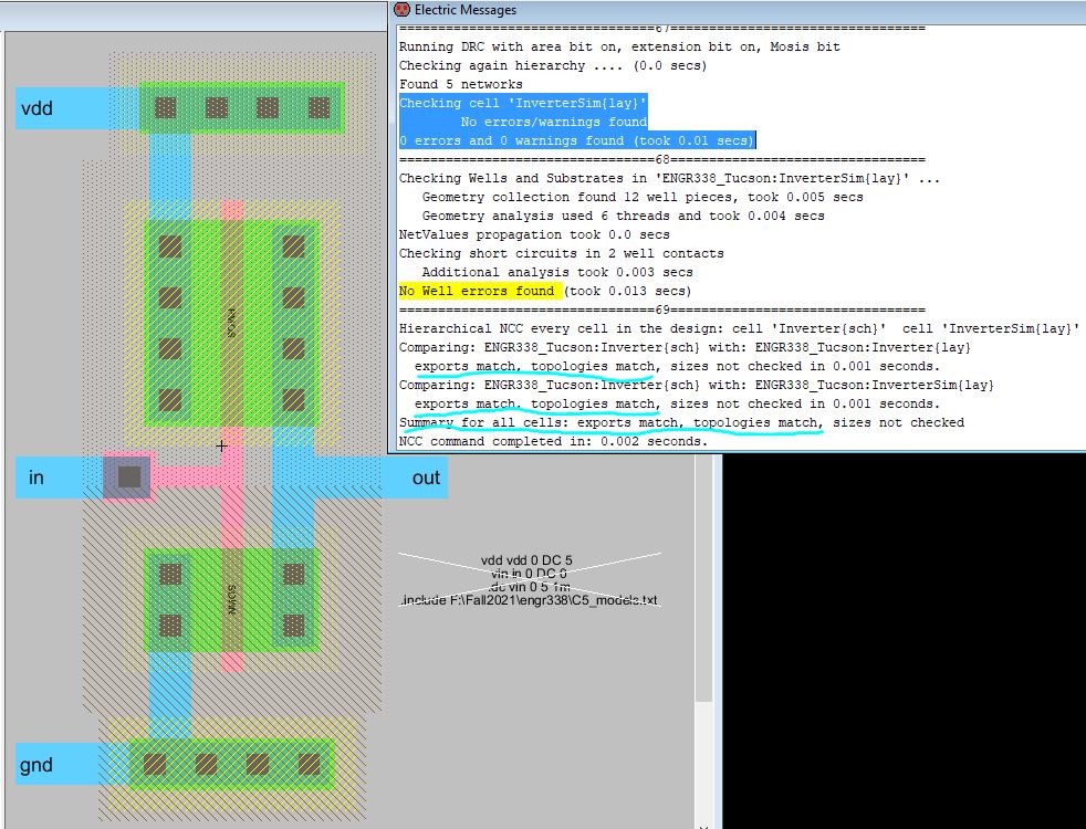
Figure 2. This is a screen-snip of the layout of the inverter using MOSFETs in Electric VLSI. The results of the DRC are displayed and highlighted in blue. The NCC results are displayed and underlined in cyan. The well check is displayed and highlighted in yellow. Note that all checks show no errors in the layout.
Next, I copied the inverter cell group to create a larger 100/50 version of the inverter, and I altered the layout to match the new sizes in the inverter as seen in Figure 3.
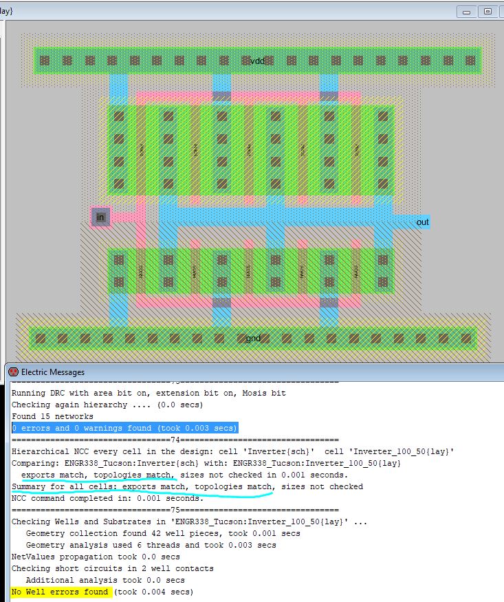
Figure 3. This is a screen-snip of the layout of the 100/50 inverter using MOSFETs in Electric VLSI. The results of the DRC are displayed and highlighted in blue, the LVS results are underlined in cyan, and the well check is highlighted in yellow. No errors are reported for any of the checks.
After that was done, I created new schematic cells for simulations of each inverter. I put a capacitor as the load, and I ran simulations at various capacitance values (100f, 1p, and 10p) for each inverter as well.
I then created a new schematic, put one of each inverter on it, each with a respective load, and I made the proper connections as shown in the second-to-last page in PDF 1. I toggled the input signals and ran simulations in the built-in ALS simulator that Electric VLSI has. After I ran that simuation, I downloaded the needed .jar file to enable the IRSIM package in Electric VLSI, and I created a new schematic with the same connections as the schematic I ran the ALS simulations from, and ran the IRSIM simulation while toggling the input signals. This can be seen on the last page of PDF 1.