ENGR338 Fall 2021
Lab 3: Layout the R-2R DAC in Electric VLSI
Name: Cheyenne Tucson
Email: crtucson@fortlewis.edu
Layout the R-2R DAC in Electric VLSI
1. Introduction
Metal-oxide-semiconductors field-effect-transistors (MOSFETs) are commonly used in the semiconductor industry; Specifically, complimentary metal-oxide-semiconductors (CMOS) in C5 technology. C5 technology can range in sizes, but the depth of the n-well cannot be easily controlled, and is usually a default measurement. The seat resistance of the C5 n-well is about 800 Ohms(Ω) per square. The resistivity, in Ω, is calculated by the formula shown below:
r = ρ(length/Area)
(EQ 1)
Here, r is the resistivity, ρ is the sheet resistance, the length is the length across the cross-section, and the area referes to the diameter of the wire.
When learning how to proficiently design circuits and components, it is good to learn good habits from the beginning. An important habit to establish for efficiently altering designs is to create repeated structures in a subcell. Once the subcell is error-free, the subcell can be reused. This will shorten the time needed to layout the design, and errors will be less likely to happen. Another good habit to form is using space-saving designs. One design that is used to save space is a serpentine layout. This is especially useful when laying out components that are in series, and when space is limited - like keeping a circuit within a 1.5 x 1.5 mm square for a silicon die.
In this lab, the schematic for the R-2R DAC that was designed in the previous lab, Designing a R-2R DAC in Electric VLSI, will be laid out using N-well resistors on the 300 nanometer scale. To do this, the habits mentioned above will be practiced.
2. Materials
- A computer with both Java, Electric VLSI, and LTSpice installed
- The .jelib library from the completed previous lab
3. Procedure
To begin, I opened up the Electric VLSI and the ENGR338 library from the last lab. I created a new schematic called "R_2R_Subcell{sch}," and I laid out the repeating strucutre in the DAC as shown in Figure 1.
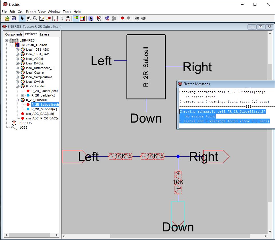
Figure 1. This is a screen-snip of the subcell with the schematic of the repeating structure of the R-2R ladder DAC, its icon, and the DRC check results. The DRC check results are highlighted in blue and report 0 errors and 0 warnings.
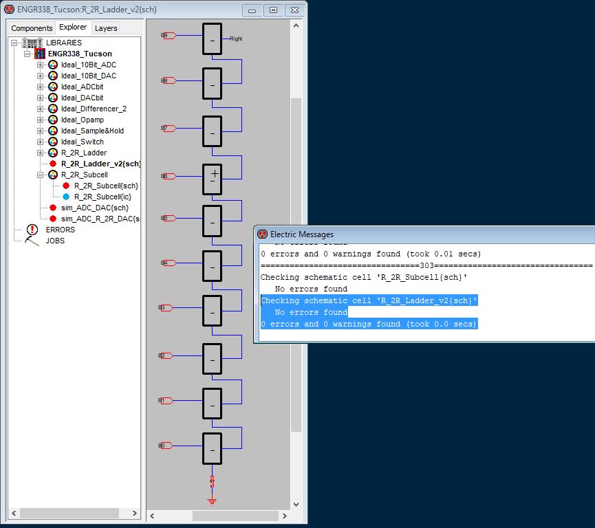
Figure 2. This is a screen-snip of the whole R-2R DAC schematic in the "R_2R_Ladder_v2{sch}" schematic that was created using the subcell from Figure 1, its icon, and the DRC check results. The DRC check results are highlighted in blue and report 0 errors and 0 warnings.
I then created an icon and ran a DRC check. Once the results came back error-free, I then created a new schematic called "R_2R_Ladder_v2{sch}," and I laid out the entire R_2R_Ladder using the subcell just created. I then ran a DRC check, and when I saw it came back error-free, I moved on to designing the layout of the DAC.
I began by creating a new layout called "R_2R_Subcell{lay}," and I adjusted the size of the "N-RWell" component's width to 15 λ and the length to 187.5 λ. I also adjusted the Well resistance to 10K. The length was found by dividing 10k Ω into 800 Ω to get the number of squares needed, and then by multiplying that result by 15 λ. I used the coordinator to place three wells evenly displaced by 25 λ, and I exported the nodes of the N-Well resistor and made the connections for the repeated structure of the R-2R ladder as shown in the first figure of the PDF seen below. I also ran both a DRC and a NCC check to make sure there were no errors in the subcell.
PDF 1. This is a PDF containing screen-snips of the following: the subcell with the layout of the repeating N-Well structure of the R-2R ladder DAC, titled "R_2R_Subcell{lay}," with the proper connections, and the results of the DRC and NCC checks are highlighted in blue; The layout of the whole DAC, titled "R_2R_Ladder_v2{lay}," that was created using the subcell just mentioned before making the proper connections, and the DRC check results are highlighted in blue; and the layout of the whole DAC, titled "R_2R_Ladder_v2{lay}," and the DRC and NCC check reports results highlighted in blue after the proper connections were made.
I then added the rest of the components to the layout, and I ran another DRC check before making the final connections. The results of the DRC are shown in the second figure in PDF 1, highlighted in blue with some nodes circled in purple to show that there were no connections made yet. After reporting 0 errors and warnings again, I added the final resistor at the end of the circuit, and I made the final connections. I ran final DRC and NCC checks to make sure everything was in order. This is shown in the last figure of PDF 1 with the results of both checks highlighted in blue. Again, no errors or warnings were reported.
Finally, I copied the simulation schematic from the first lab to a new one, and I replaced the DAC with the icon from the "R_2R_Ladder_v2{sch}," so I could run the simulation in LTSpice.
4. Results
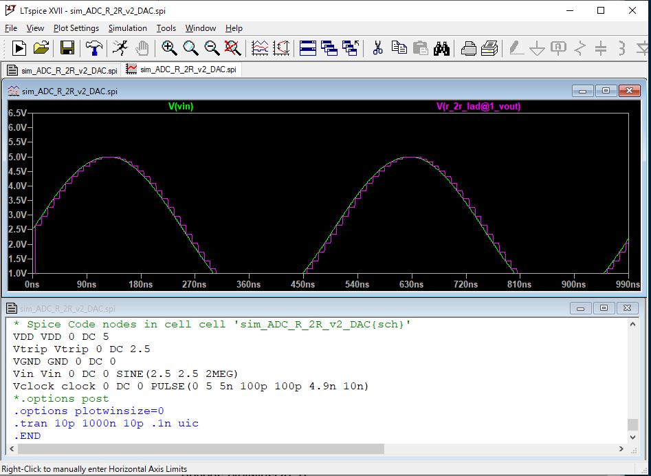
Figure 3. This is a screen-snip of the LTSpice simulation results. The analog input, in green, is plotted with the digital output, in purple.
5. Discussion
The simulated results were as to be expected. I noticed the results are the same as what were seen in the previous lab (which is great!) I enjoyed learning more about how the PMOS transistors can be used as resistors. This was more good practice with designing physical layouts in Electric VLSI. By reinforcing these useful habits early on, I belive that laying out larger circuits in VLSI software will be much more efficient for the future projects I may work on.