Creating K-Maps for each of the lights, we get:
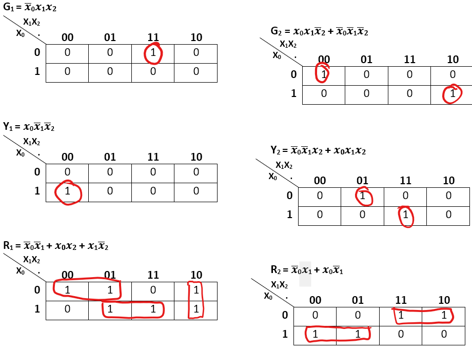
Figure 1: K-Maps used to simplify logic from the truth table.
From the K-Maps we get the following logic:
G1 = X0X1X2
Y1 = X0X1X2
R1 = X0X1 + X0X2 + X1X2
G2 = X0X1X2 + X0X1X2
Y2 = X0X1X2 + X0X1X2
R2 = X0X1 + X0X1
Here's the code for the traffic light module:
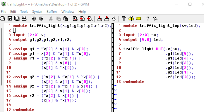
Figure 2: Traffic Light module.
The way the code has been set up, traffic light 1 is simulated with leds 5-3 starting with green, traffic light 2 is represented with leds 2-0 starting with green and the inputs are using switches 2-0 as shown below:
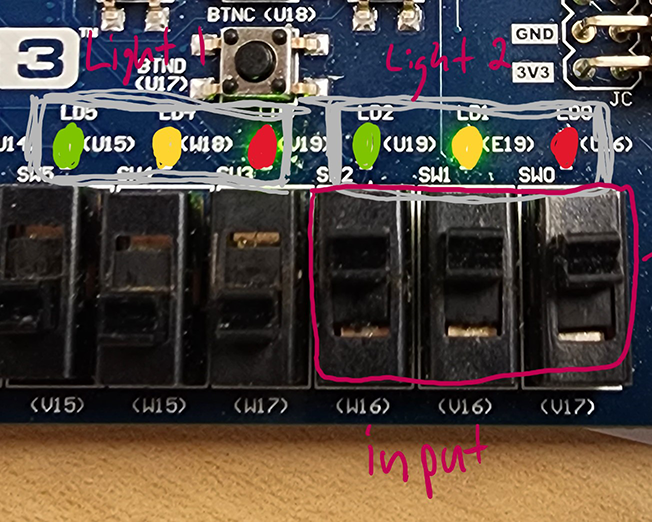
Figure 3: FPGA labeled with inputs and outputs.
Here is a YouTube Link demonstrating the FPGA programmed with the logic.
Even Bit Parity Checker and Generator:
An even bit parity checker is meant to check for errors due to noise from the parity generator.
A parity generator is to display whether the toggled bits are even, it will display when the bits are uneven.
Here's the code for the even bit parity generator and checker modules:
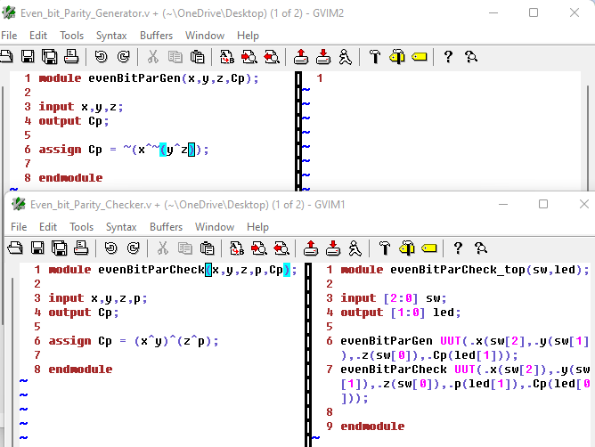
Figure 4: Code for the Even Bit Parity Generator and Checker.
Here's a diagram for the FPGA programming:
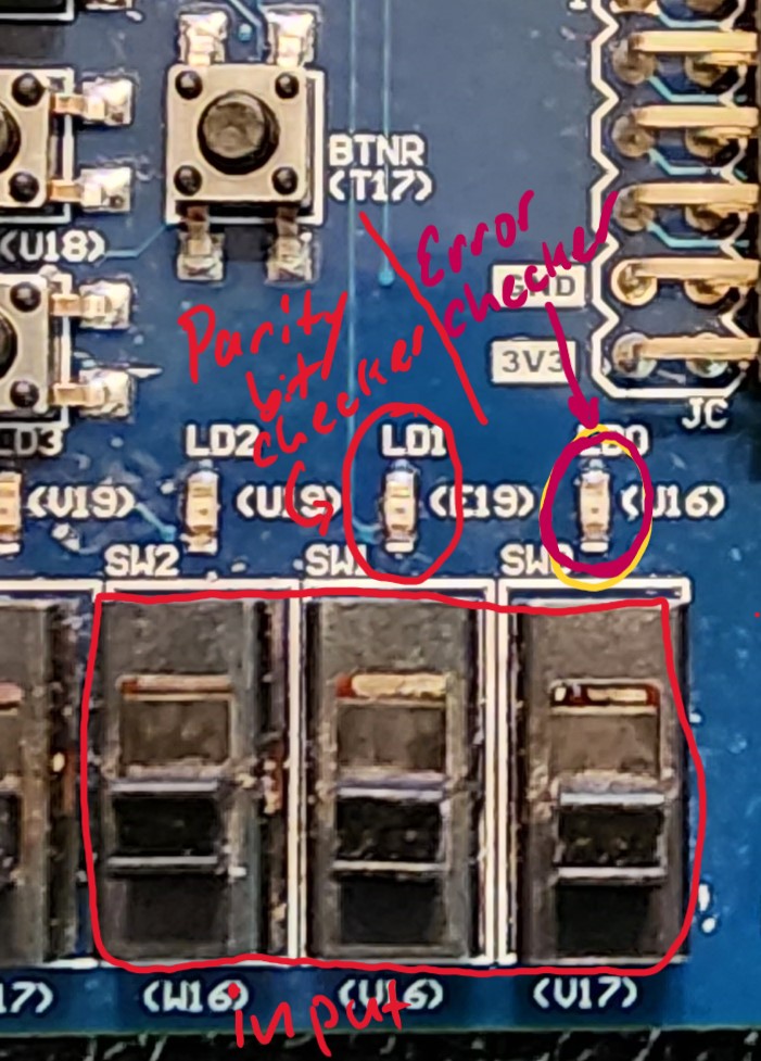
Figure 5: Diagram of the FPGA inputs and outputs.
Switches 0 through 3 represent the bits being passed through. So anytime an odd number of bits have been toggled, led 1 would light to make an even set of bits. Led 0 will light if and odd number of bits are detected after the even bit parity generator has corrected to an even number of bits indicating an error with the generator.
However, since there is very little to no chance for error in such a simplified system, led 0 should never light up indicating no error with the generator.
Here is a Youtube link demonstrating the FPGA programmed and its logic.