CE 433-2 Lab 2023 Spring
Lab 3: Seven Segment Display and Others
Name: Vann Montoya
Email: bvmontoya@fortlewis.edu
More about FPGA - Seven Segment Display and Others
Introduction
The purpose of this lab is to demonstate programming the FPGA, using switches, LEDS and 7-segement display.
Materials and Methods
Vivado
FPGA
Results
Task 1.
Using Verilog and Vivado to demonstrate the following combinational
logic blocks in both simulation and on the board (switches/leds):
1) Inverter 2) 2-bit full adder 3) 8-input And 4) 4-1 MUX (can use an embedded condition: y=s1?(s0?d3:d2):(s0?d1:d0))
Note the Verilog conditional operator: (condition ? value_if_true : value_if_false)
1) Inverter
The inverter is to invert the signal of an input. When the input is 0, the inverter will invert it to 1 and vise versa.
Here is the code for the simulation:
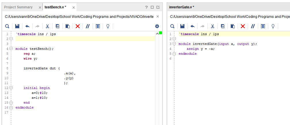
Figure 1: Inverter simulation code module and test bench.
Here is the results from the simulation:
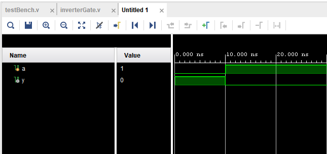
Figure 2: Simulation results from the inverter.
Here is the code for programming it to the FPGA:
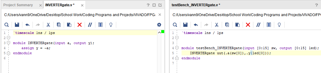
Figure 3: Code for programming the FPGA inverter.
Here is the Youtube link demonstating the FPGA programmed with the inverter.
2) 2-bit Adder
A 2-bit adder will add two inputs together such as 0 + 0 = 00, 0 + 1 = 01, 1 + 0 = 01 and 1 + 1 = 10.
Here is the code for the 2-bit adder:
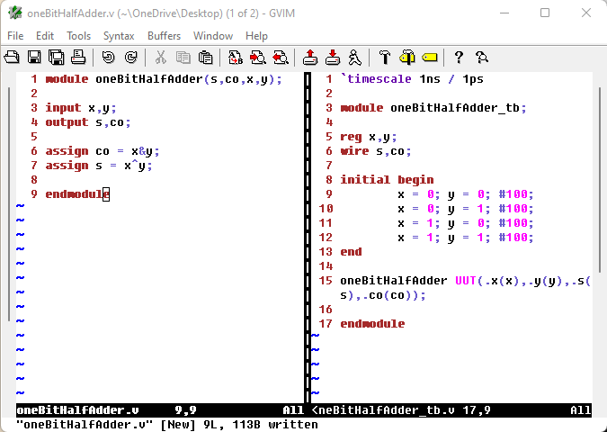
Figure 4: Code for the 2-bit adder and test bench.
Here are the results from the simulation:
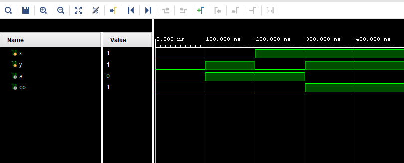
Figure 5: Simulation results from the 2-bit adder.
Here is the code for programming the FGPA with the 2-Bit Adder:
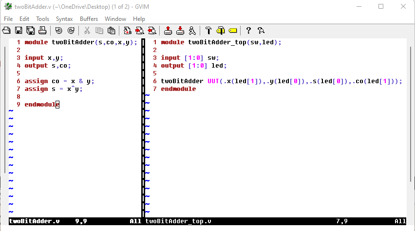
Figure 6: Code for programming the FPGA.
Here is the Youtube link demonstrating the logic implemented on the FPGA.
3) 8-input
The purpose of this program is to accept 8 individual inputs.
Here is the code for the simulation run:
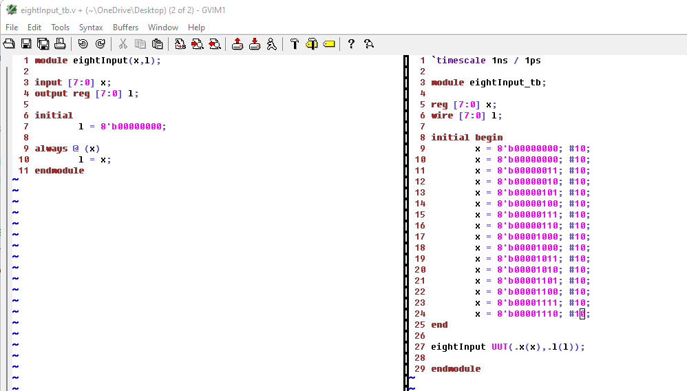
Figure 7: Code for the 8-input simulation.
Here is the results from the simulation:
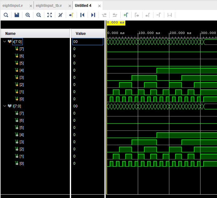
Figure 8: Simulation results from the 8-input.
Here is the code for programming the FPGA for the 8-inputs:
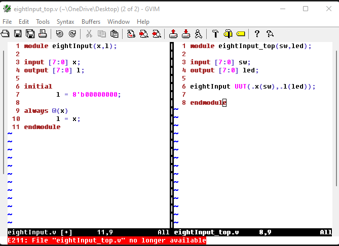
Figure 9: Code for programming the FPGA with the 8-inputs.
Here is the Youtube link demonstrating the FPGA programmed.
4) 4-1 Mux
The purpose of a 4-1 multiplexer is to allow a combination of two inputs to allow a specific signal through.
Here is the simulation code for the 4-1 MUX:
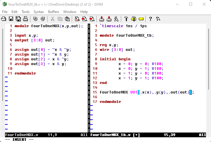
Figure 10: Code for the 4-1 MUX simulation.
Here are the results from the simulation:
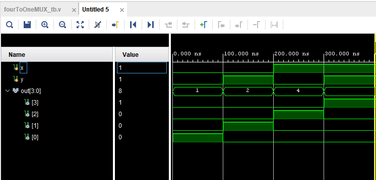
Figure 11: Results from the 4-1 MUX simulation.
Here is the code for programming the FPGA:
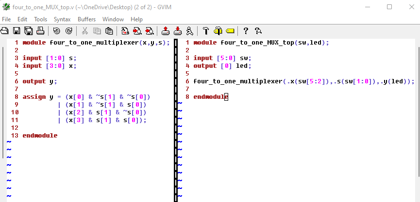
Figure 12: 4-1 MUX code for the FPGA.
Here is the Youtube link demonstrating the FPGA programming.
Task 2: Using
Verilog and Vivado to design a 'Running LED' program on the FPGA board.
Use 4 LEDs on the board, turn on each of them for 1 second one-by-one.
The purpose of this task is to program the FPGA to make the LEDs from 0-3 to turn on sequentially from the first to the next.
Here is my code for the running LED program:
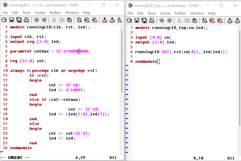
Figure 13: Code for the running LEDs.
The way the code is set up is based on if statements.
The first if statement is to check either the rest switch has been
toggled. If it has then reset the counter to zero and the LEDs back to
the first.
The second if statement is to check if the counter has reached the max
threshold, then switch the LED to the next and reset the counter.
The last statement is to increment the counter and keep the LED status the same.
For this program, the constraints file needs to be update to include the clock signal:
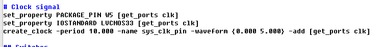
Figure 14: Updated constraints file to include clock signal.
Vivado will compile everything and even upload the bit-stream file to
the FPGA board, however, when programmed to the board, only the first
LED will light up and will not update.
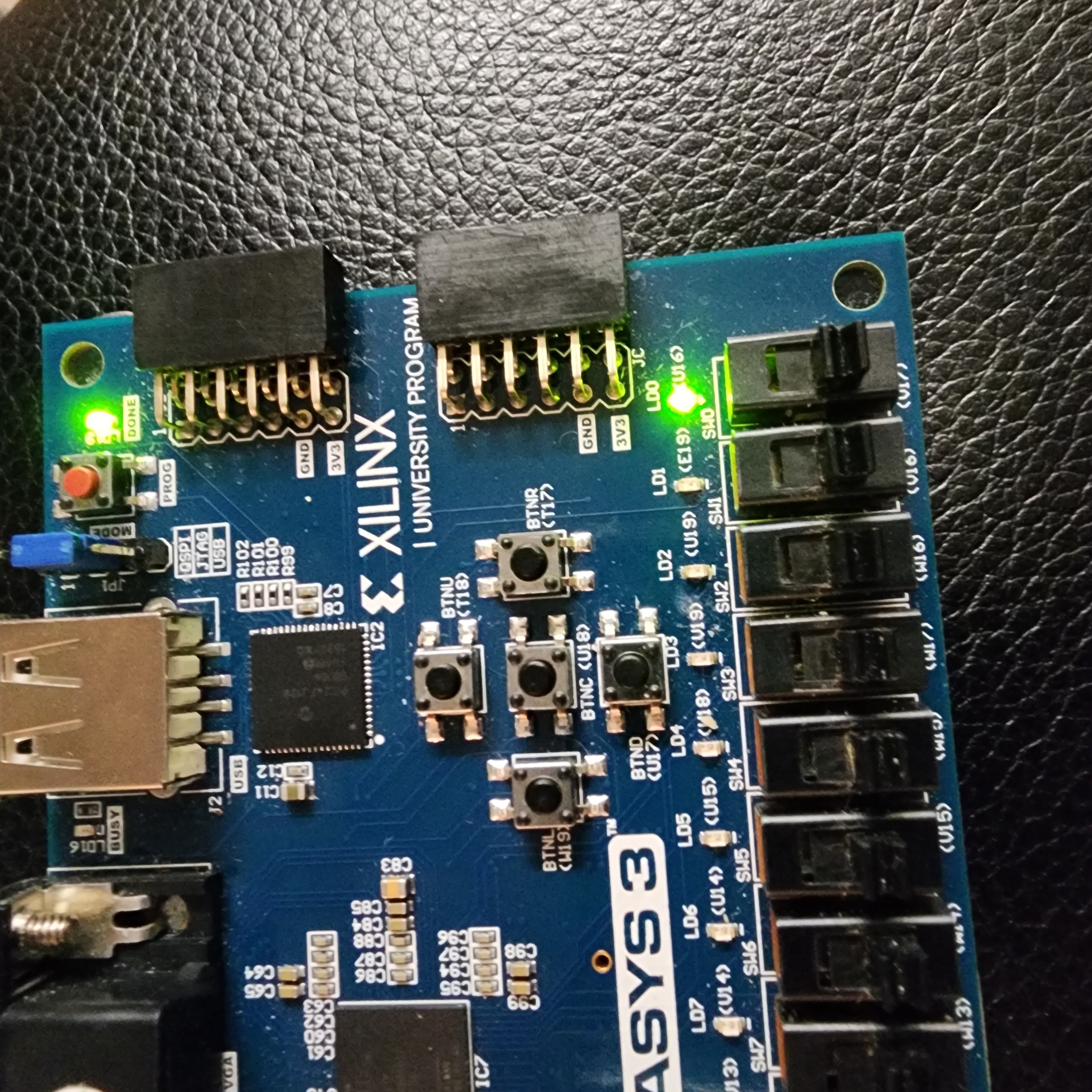
Figure 15: FPGA board uploaded with the runningLEDs program, however, only first LED stays lit up.
Not sure what is causing this issue, however, I think it is due to the
counter not incrementing and remaining in the first state.
Task 3: Interface
the switches with the 7-segment display on the board. (make sure you
have the '##7 segment display' part in your constraint file uncommented)
For this task, we are to program the FPGA board to use the 7-segment
display to display the binary decimal equivalent of bits represented by
switches 0-3.
For example, switches 0-3 represent each bit of a 4-bit binary number,
so if switches 0 and 2 were toggled, then that would represent 0101 or
5 in decimal which would be displayed by the 7-segment display.
Here is the code for the seven segment display:
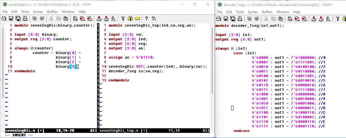
Figure 16: Code for the FPGA programming of the 7-segment display.
Here is the Youtube link demonstrating the FPGA programmed with the 7-segment display.