CE 433-2 Lab 2023 Spring
Lab 2: Introduction to FPGA
Name: Vann Montoya
Email: bvmontoya@fortlewis.edu
Introduction to FPGA
Introduction
The purpose of this lab is to introduce programming the FPGA using Vivado.
Materials and Methods
FPGA board
Vivado
Results
Tasks:
Task 1.
Go through all the steps in this lab instruction, report your code,
simulation results, and the on-board verification results. (30 points)
First part was to create an And Gate simulation using Vivado.
Here is the code for the andGate module and its test bench.
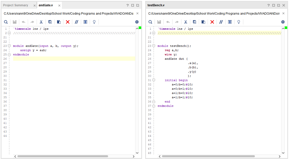
Figure 1: And Gate module and test bench code used in Vivado simulation.
Running the simulation resulted in the following:
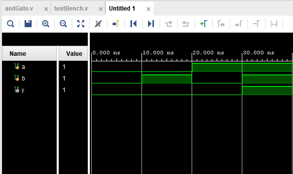
Figure 2: Simulation results from AndGate testbench.
As you can see, when inputs a and b are both 1 then out y becomes 1.
Now we can move onto programming the physical FPGA board.
Here is the andGate module for the FPGA.
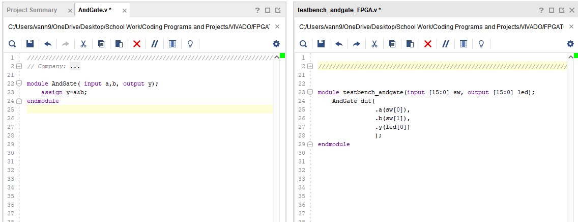
Figure 3: The code for programming the FPGA.
Once the code has been uploaded to the FPGA, now switches 0 and 1 will act as inputs and led 0 will act as the output.
So if either switch or both switches are off, then the led will not light because of the AND gate logic.
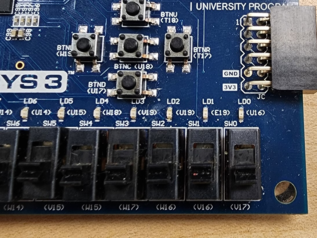
Figure 4: Displaying both switches 0 and 1 are off, so led 0 will be off.
Now if both switches were to be switched on, then the led should light.
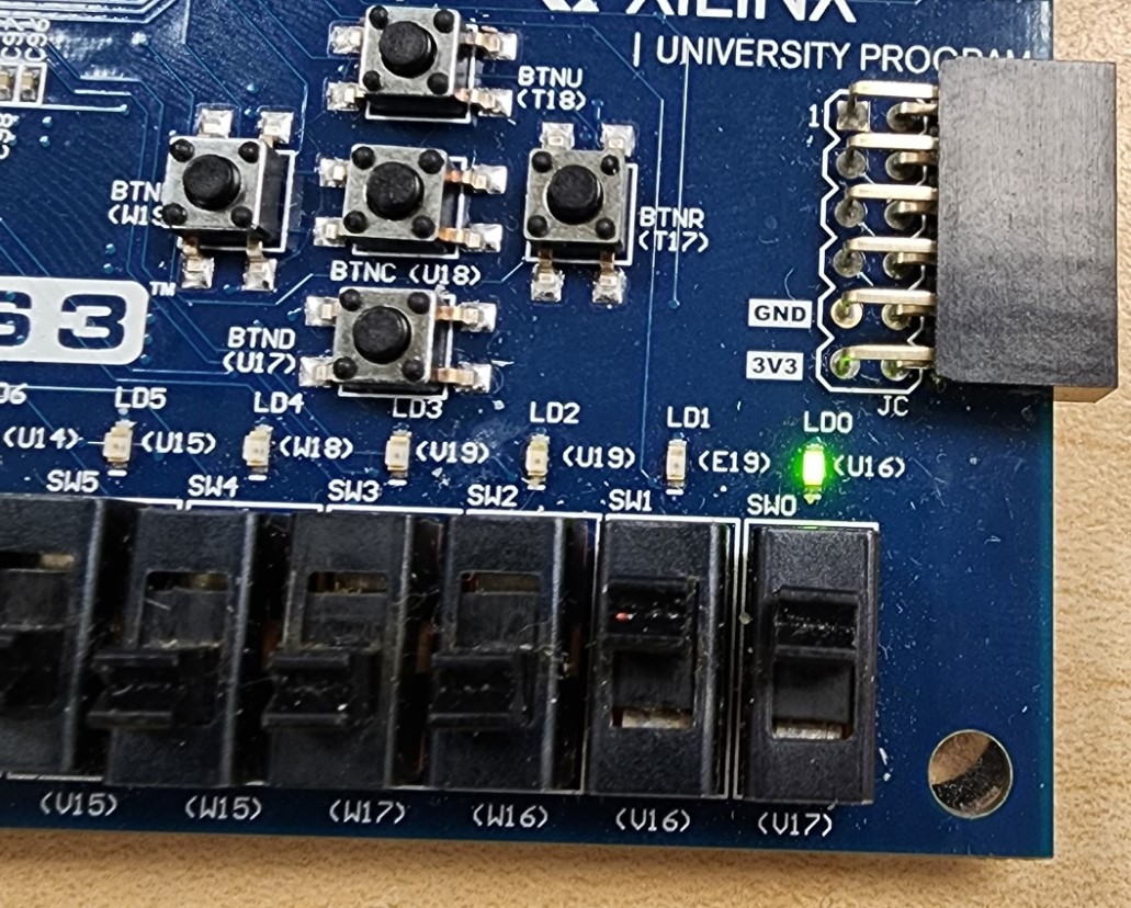
Figure 5: Displays that when both switches 0 and 1 are switched on, then led 0 is on due to the AND Gate logic.
Task 2. Use the same procedure to create XOR and OR gates. Run simulations to verify the logic. (30 points)
For the simulations, code was written for each gate.
Here is the code and test bench for the OR gate.
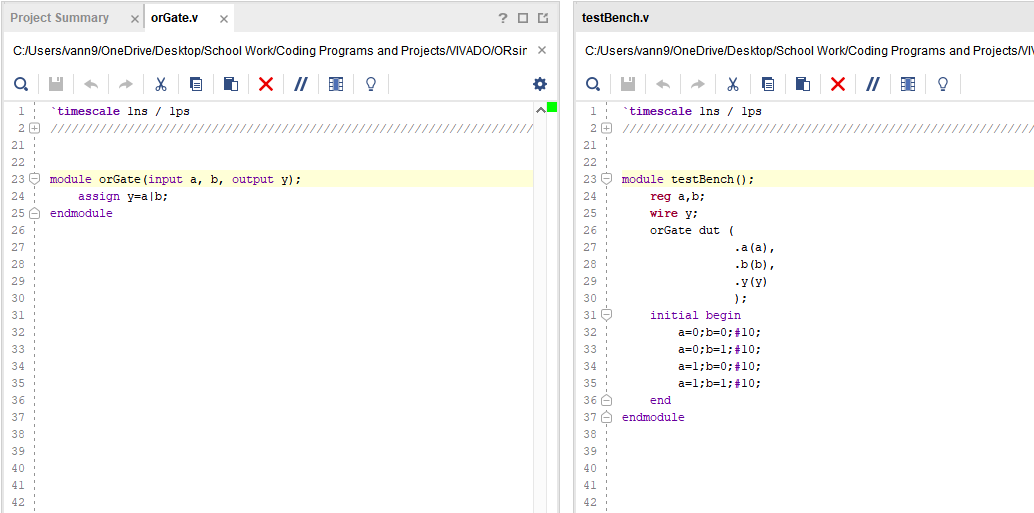
Figure 6: Code for the OR gate and test bench.
Here is the results from the simulation. As you can see, when either switch 0 or 1 has been flipped, output y is on.
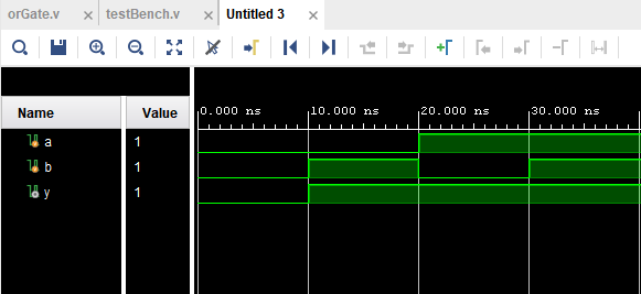
Figure 7: Simulation results from or gate.
Here is the coding for the XOR gate and test bench.
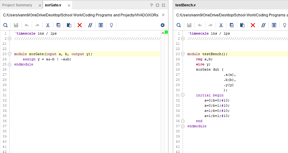
Figure 8: XOR coding for the logic gate and test bench.
Here are the simulation results from the XOR gate.
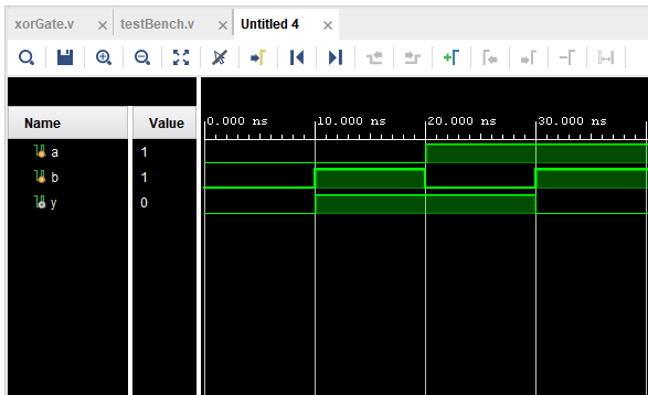
Figure 9: Results from the simulated XOR gate. Here you can see that when only one of the inputs have been toggled but not both, y is 1.
Task 3. Use both the volatile and nonvolatile methods (QSPI) to program your FPGA. Show videos for the demonstrations. (40 points)
Here is a link to a Youtube video demonstrating the FPGA's on board memory.
It shows a programmed OR logic gate that is still consistant even after powering off the FPGA.