CE 433-2 2023 Spring
Report 3: Combinational
Logic Blocks
Name: Vann Montoya
Email: bvmontoya@fortlewis.edu
Combinational
Logic Blocks
Introduction
The purpose of this assignment is to further familiarize ourselves with
Vivado and programming the FPGA board using combinational logic blocks.
Materials and
Methods
Vivado
FPGA board
Results
Tasks
1.
Repeat the simulation of Half Adder and Full Adder in Section 1. (10
points)
Here is my code for both the one bit half adder module and test bench:
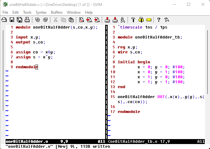
Figure 1: One bit half adder module
and test bench
Running the simulation for the one bit half adder resulted in the
following:
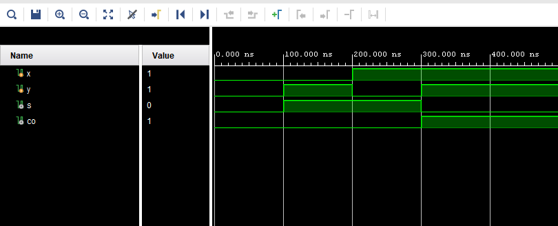
Figure 2: Simulation
results from the one bit half adder.
Here is my code for the one bit full adder module and test bench:
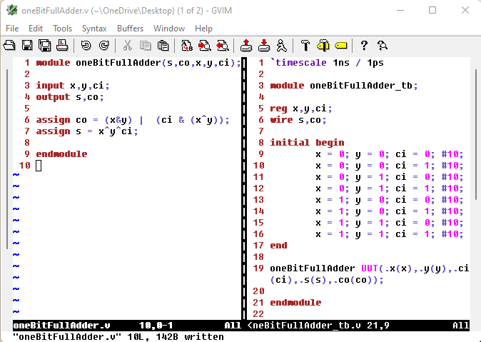
Figure 3: One
bit full adder module and test bench.
Running the simulation for the one bit full adder module resulted in
the following:
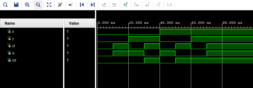
Figure 4: One
bit full adder simulation results.
2. Design the testbench for the comparator in Section 2
and show the simulation results. (10 points)
For this portion, we are creating a bit comparator that indicates
whether the first bit is greater than, equal to or less than the second
bit.
We will be using two inputs x and y and three outputs g, (greater than)
e, (equal to) and l (less than) for each of the conditions.

Figure 5: Truth table for the bit
comparator.
Here is my code for the one bit comparator module and test bench:
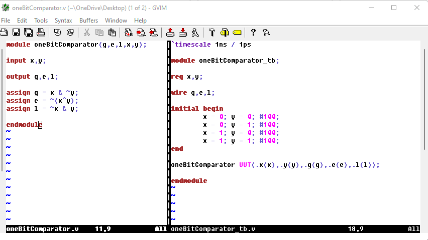
Figure 6: One bit
comparator module and test bench.
Here are the results from the one bit comparator simulation:
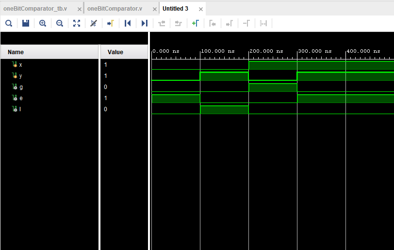
Figure 7: Simulation
results of the one bit comparator.
3. Design the testbench for the 4-bit comparator
in Section 3 and show the simulation results. (10 points)
Now we will create a 4-bit comparator.
Here is my code for the 4-bit comparator module and test bench:
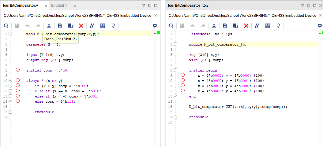
Figure 8: 4-bit comparator and
test bench code.
Here are the results from the simulation:
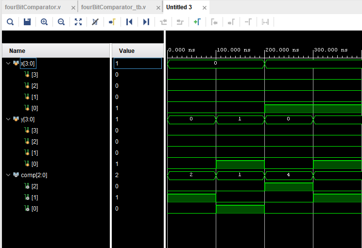
Figure 9: Results from the
4-bit comparator simulation.
You can see that as the simulation runs we get the following truth
table:
x
y comparator
0000 0000 010
0000 0001 001
0001 0000 100
0001 0001 010
Which makes sense because when:
x > y, the comp should be 100
x = y, the comp should be 010 and
x < y, the comp should be 001,
which is eactly what we see.
4.
Implement a 2-bit comparator on the Basys 3 board. Use sw as inputs and
led as outputs. (10 points)
Now
we want to create a two bit comparator and implement it to the FPGA
board.
Here is the code for the 2-bit comparator module and top module:
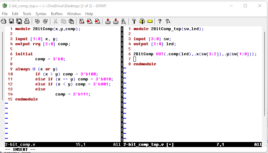
Figure 10: 2-bit comparator
module.
The FPGA board has been programmed such that x is represented by
switches 2 and 3, y is represented by switches 0 and 1, led 2
represents x > y, led 1 represents x = y, and led 0 represents x
< y.
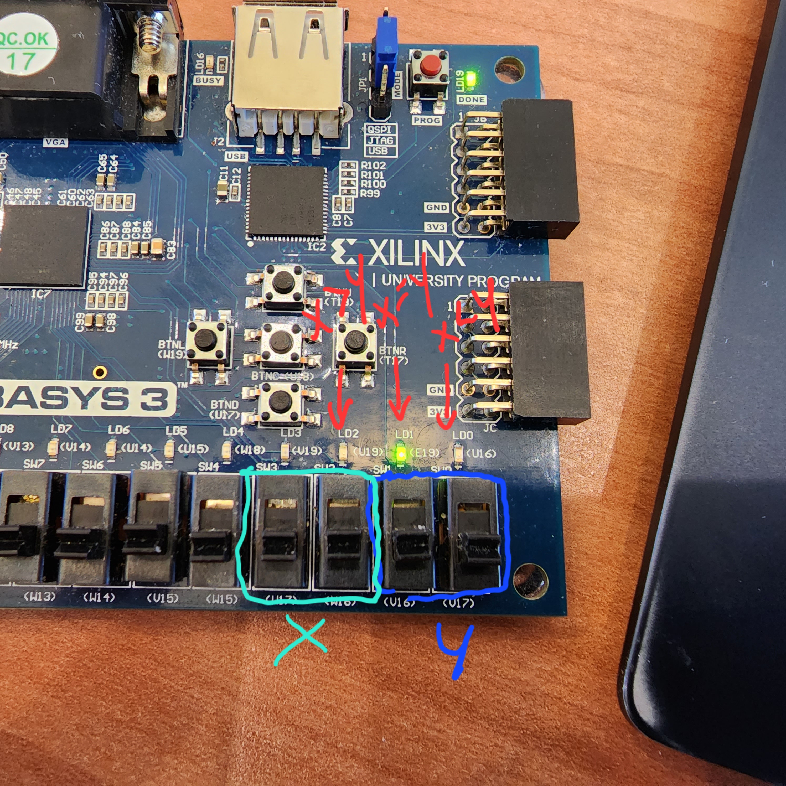
Figure 11: Diagram of the FPGA
board with switches and leds labeled.
Here is a link to the Youtube video demonstrating the
FPGA logic.
5. In Section 4, design the testbench for the decoder and verify the
logic in simulation (use the Dataflow modeling method). (10 points)
Here
is my code for both the module and test bench:
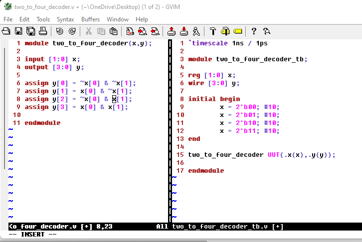
Figure 12: Two-to-four decoder
module and test bench.
Here are the results from the simulation:
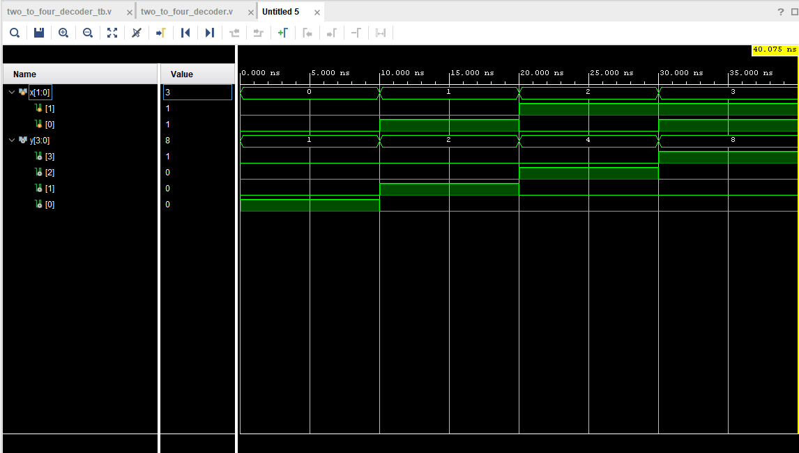
Figure 13: 2-to-4 decoder
simulation results.
6. In Section 5, for the 8x3 priority encoder, find Q2 and Q1, build
the module and verify the logic using simulations. (10 points)
First
we need to find Q1 and Q2 from this truth table for the 8x3 priority
encoder:
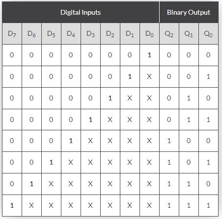
Table 1: Truth table for a 8x3
priority enconder.
We get the boolean expression for:
Q0 = !D6•(!D4•!D2 • D1 + !D4•D3 + D5) + D7
Q1 = !D5•!D4•(D2 +D3) + D6 + D7
Q2 = D4 + D5 + D6 + D7
Q1 = Σ(2,3,6,7)
= !D7•!D6•!D5•!D4•!D3•D2 + !D7•!D6•!D5•!D4•D3 + !D7•D6 + D7
= !D7•(!D6•!D5•!D4•!D3•D2 + !D6•!D5•!D4•D3 + D6) + D7
= (!D6•!D5•!D4•(!D3•D2 +D3) + D6) + D7
= (!D5•!D4•(D2 +D3) + D6) + D7
Q2 = Σ(4,5,6,7)
= !D7•!D6•!D5•D4 + !D7•!D6•D5 + !D7•D6 + D7
= !D7•(!D6•(!D5•D4 + D5) + D6) + D7
= ((D4 + D5) + D6) + D7
= D4 + D5 + D6 + D7
Now we can try and implement it into Vivado.
Here is my code for the module and test bench:

Figure 14: 8x3 Priority Encoder module and test bench code.
Here are the results from the simulation:
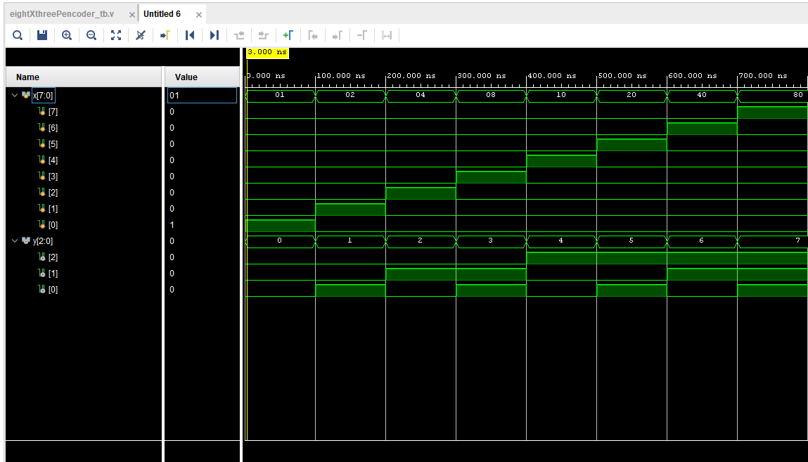
Figure 15: 8x3 Priority Encoder simulation results.
7. In Section 6, implement a 4-1 multiplexer on your Basys 3 board.
Show embedded Youtube video demonstration on your report. (10 points)
A 4-1 multiplexer is designed so that by only using two switches (or
inputs), you are able to control which signal is passed through as the
output.
Here is the code for my module and top module:
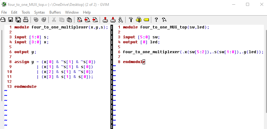
Figure 16: 4:1 multiplexer module and top module.
The code was written such that switches 0 and 1 are the toggle switches
that select which signal is allowed to pass through as the output and
switches 2 through 4 are the input signals.
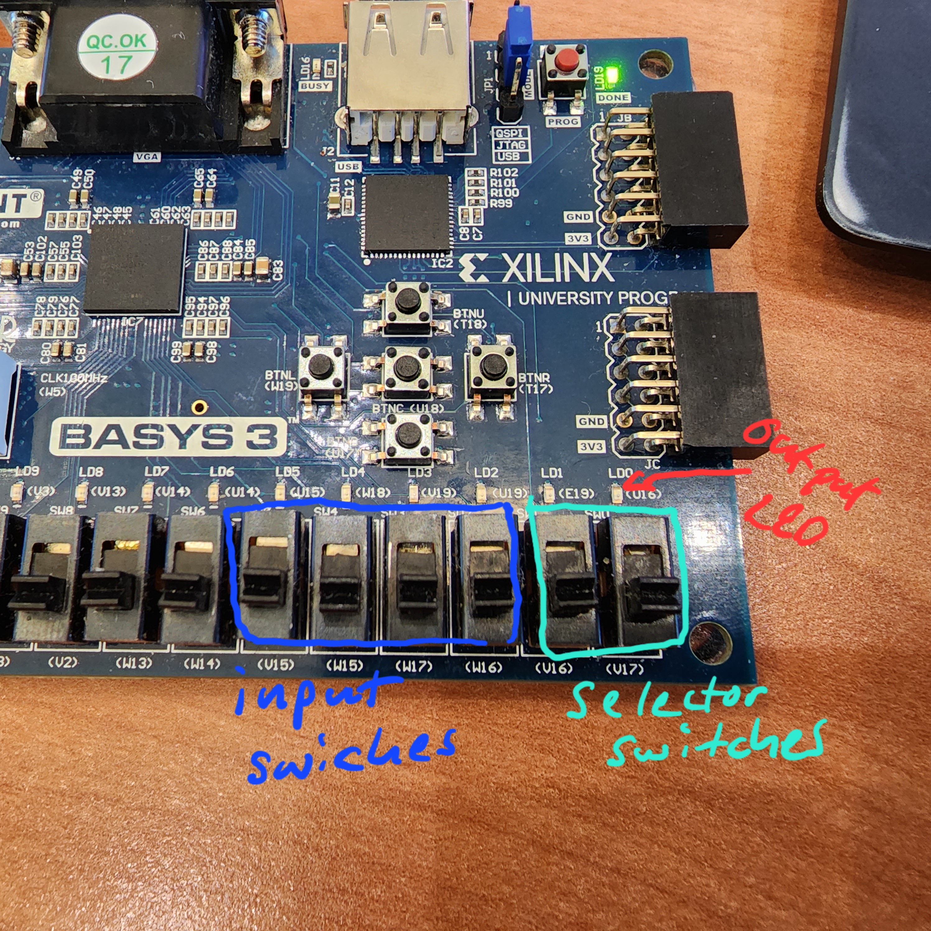
Figure 17: Diagram of the FPGA board with switches and led labeled.
Here is the Youtube video link demonstrating the FPGA board logic.
8.
Design/verify an even parity generator and checker in simulation
respectively. Implement an even parity checker on your Basys 3 board -
use sw as inputs, use leds as output indicators. Show embedded Youtube
video demonstration on your report.(10 points)
An even bit parity generator will sense when the number of bits from the input is even or not.
In this case, I've created a 3-bit even parity generator.
Here is the code for the modules:
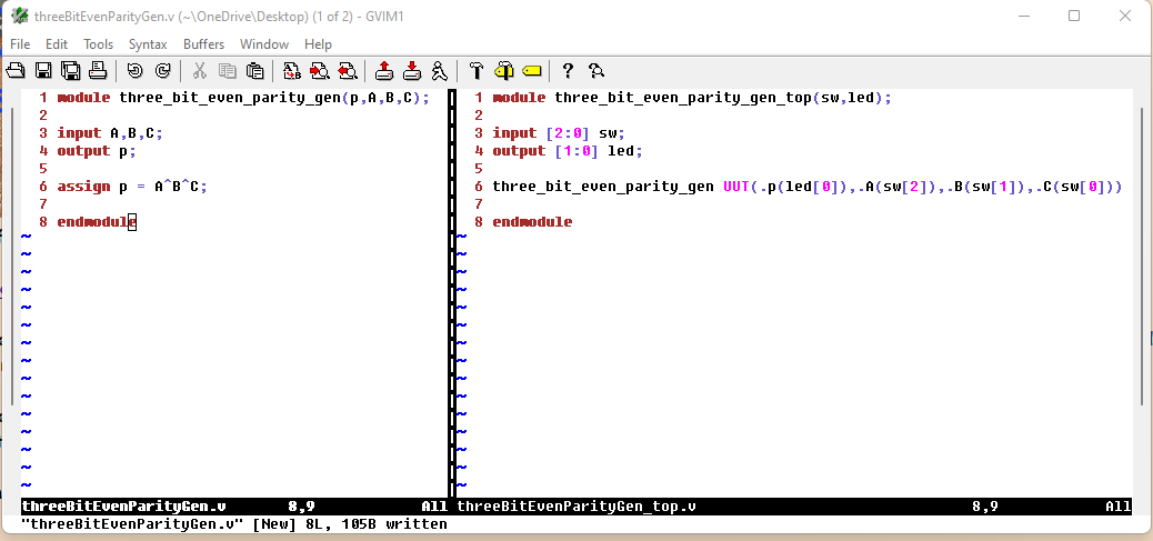
Figure 18: Code for the 3-bit even parity generator.
Now the FPGA has been programmed such that switches 0 through 2
represent individal bits and LED 0, when lit up, indicates an odd
number of bits.
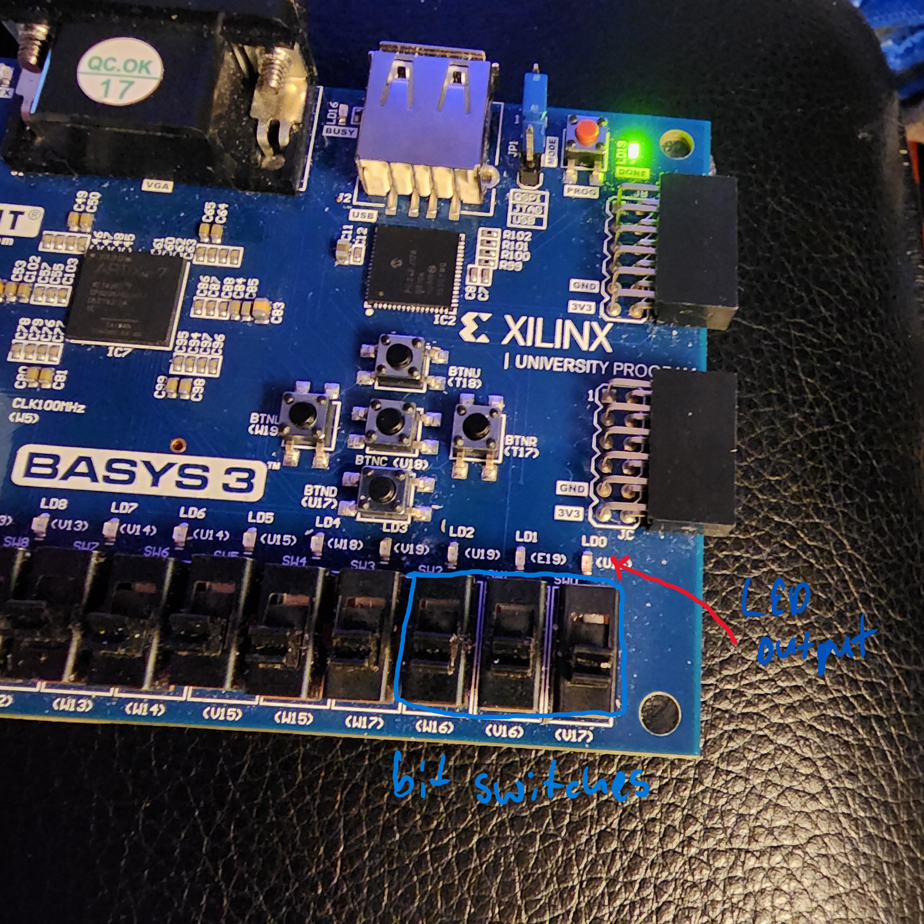
Figure 19: Diagram of the FPGA inputs and outputs.
Here is the Youtube link demonstrating the FPGA logic.
9.
Implement the design in Section 8 and Section 9 on your Basys 3 board.
Show embedded Youtube video demonstration on your report.(20 points)
First part is creating the home alarm from the previous week and improving it by adding a display using the 7-segment display.
Here is the code for home alarm module, top module and 7-segment display:
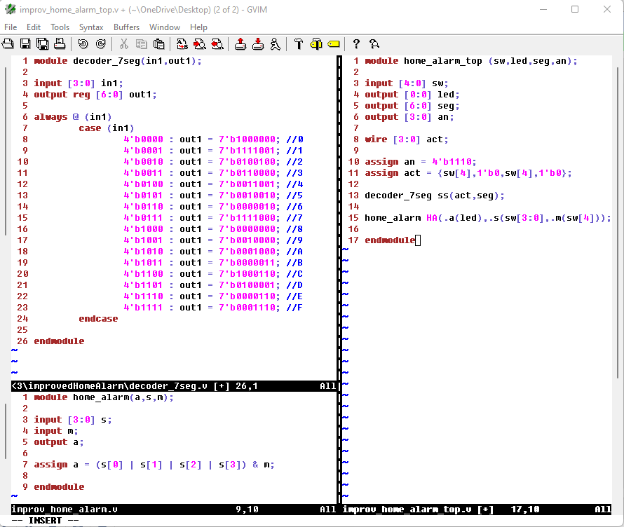
Figure 20: Code for the improved home alarm.
The FPGA is programmed to mimic a very basic home alarm system such
that there is one switch which arms the system and four switches that
act as doors/window sensors that when tripped will set off the alarm
which will be represented by LED 1.
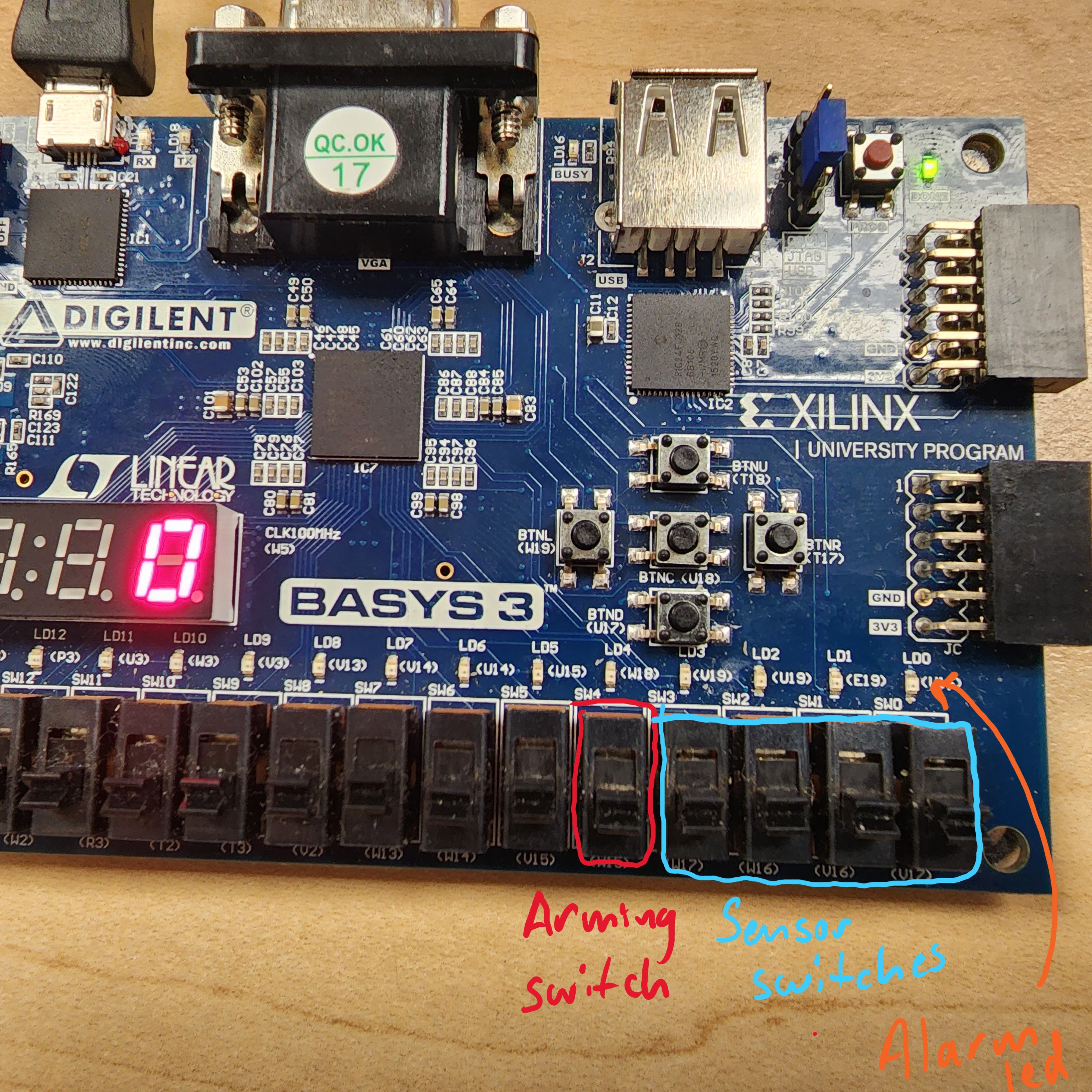
Figure 21: FPGA board diagram with switch and led labels.
The 7-segment display is used to indicate when the system is armed. It will display an 'A' when armed.
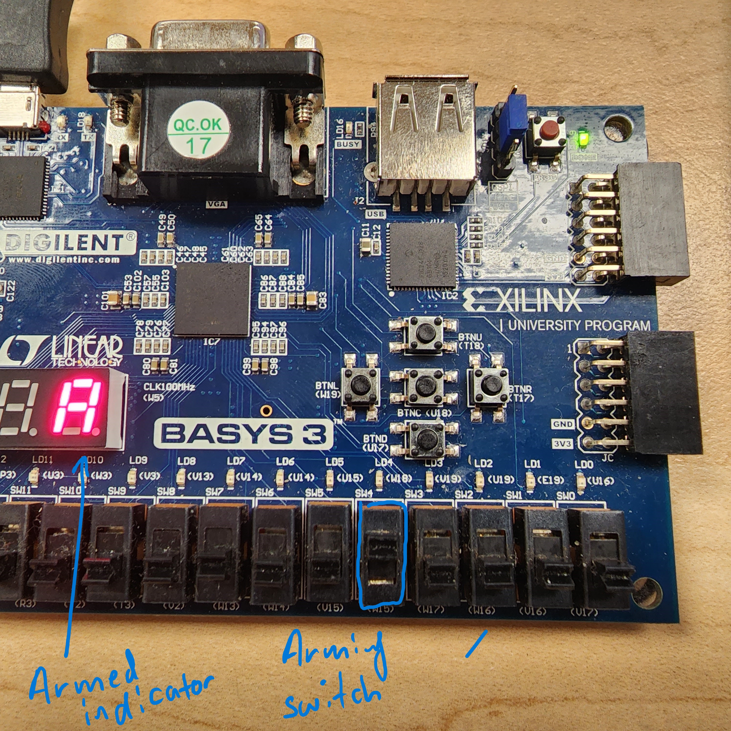
Figure 22: FPGA board with the arming switch toggled and 7-segment displays.
Here is the Youtube link demonstrating the FPGA board logic.
Next we are improving the car parking system. The purpose of the
program is to count the number of toggled switches. In this case we are
adding the 7-segment display to show the numeric number in addition to
the leds representing binary.
Here is the code:
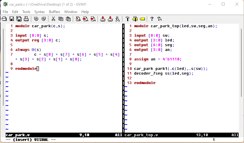
Figure 23: Car park module code.
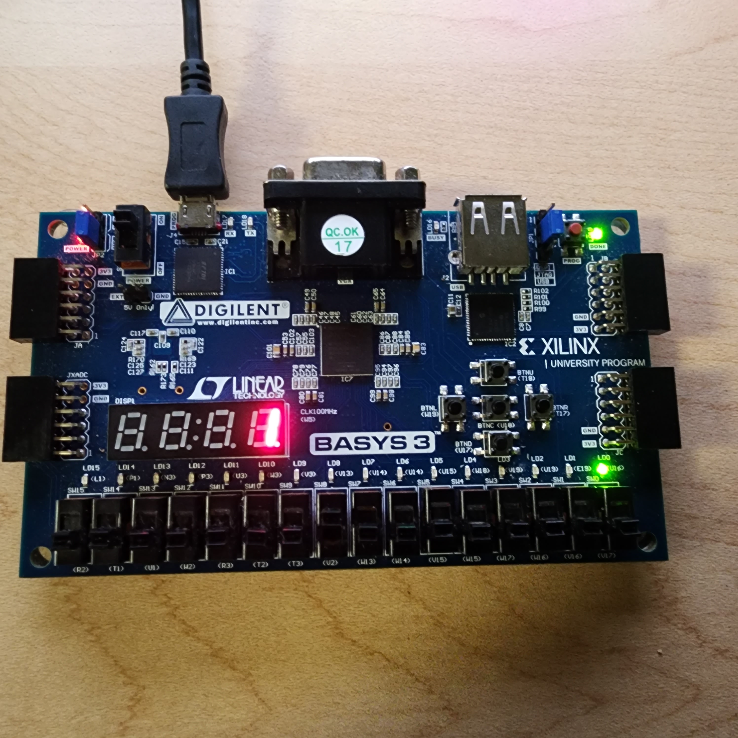
Figure 24: FGPA board programmed.
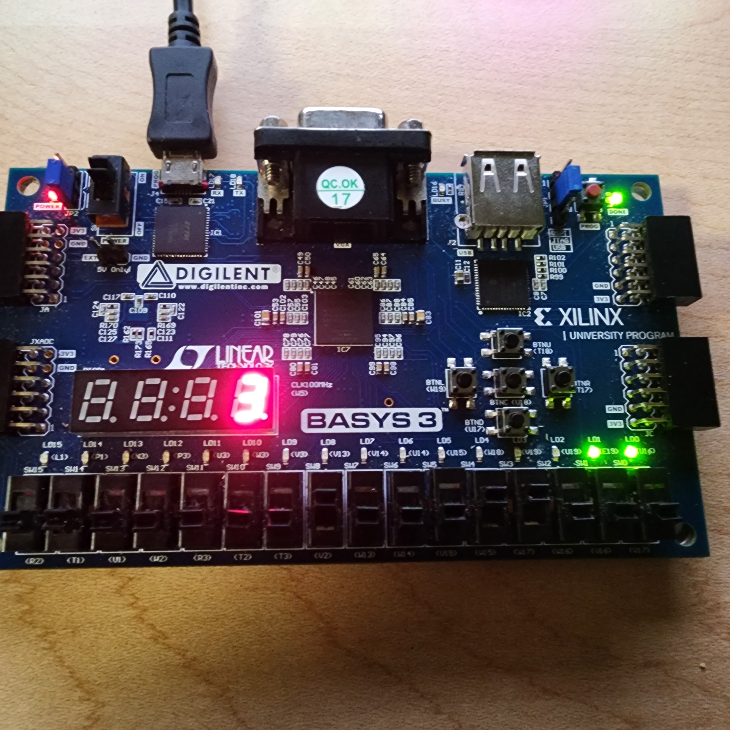
Figure 25: FPGA board programmed showing a higher count.
Here is the Youtube link demonstrating the FPGA logic.
Discussion