CE 338 Lab 2023 Fall
Lab 7: Using Buses in ElectricVLSI
Name: Vann Montoya
Email: bvmontoya@fortlewis.edu
Using Buses in ElectricVLSI
Introduction
The purpose of this lab is to use ElectricVLSI to build a ring oscillator using buses and multi-bit gates.
Materials and Methods
ElectricVLSI
LTSpice
Results
Task 1: Build and simulate a Ring oscillator. (20 points)
First, we want to build the ring oscillator, pulling from our premade inverters made in lab 4.
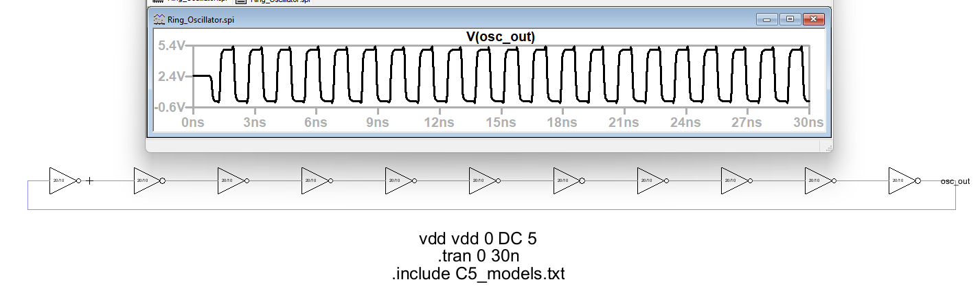
Figure 1: The Ring Oscillator Created Using our Premade Inverters from Lab 4.
Now, we want to create the ring oscillator but using buses.
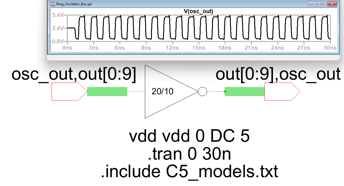
Figure 2: The Ring Oscillator Created Using our Premade Inverter from Lab 4 and with Buses.
Next, the layout. Use buses is not an option in the layout view. Please explain why in your report.
Buses
are not an option in the layout view because the layout is exactly how
the components are layed out thus each individual inverter must have
connections.
Finally, we want to create the layout for the ring oscillator.
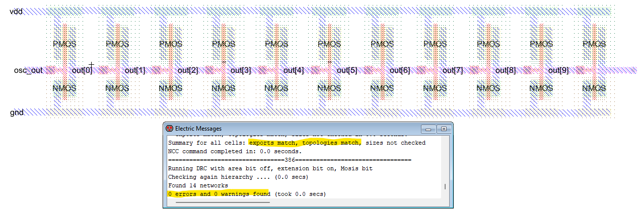
Figure 3: The Ring Oscillator Created in Layout View with No Errors.
Task 2: Design an 8-bit AND gate. (20 points)
First, we want to create an AND gate using the NAND and INVERTER configurations.
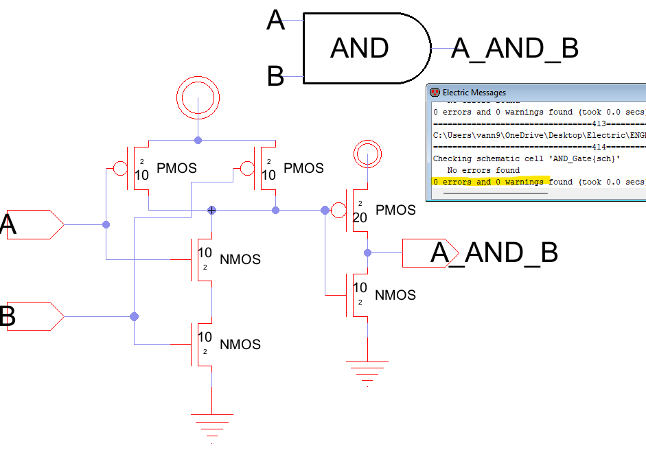
Figure 4: The AND Gate Schematic and Icon with No Errors.
We need to create the layout now.

Figure 5: The AND Gate Created in Layout View with No Errors.
Next, we create the 8-Bit AND Gate using buses.
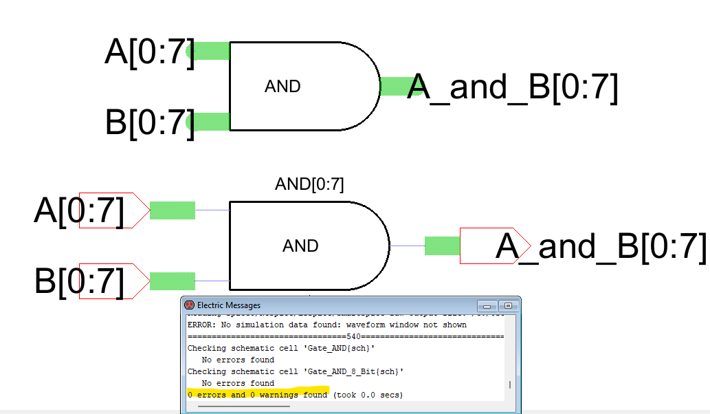
Figure 6: The 8-Bit AND Gate Schematic and Icon with No Errors.
We want to run the simulation to see if all is working.
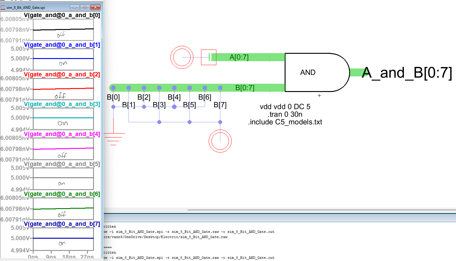
Figure 7: The 8-Bit AND Gate Simulation and Results.
Lastly, we need to build the 8-Bit AND Gate Layout.
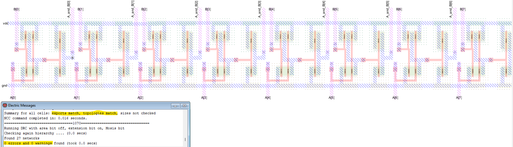
Figure 8: The 8-Bit AND Gate Layout with No Errors.
Task 3: Design an 8-bit OR gate. (20 points)
First, we need to build the OR Gate schematic.
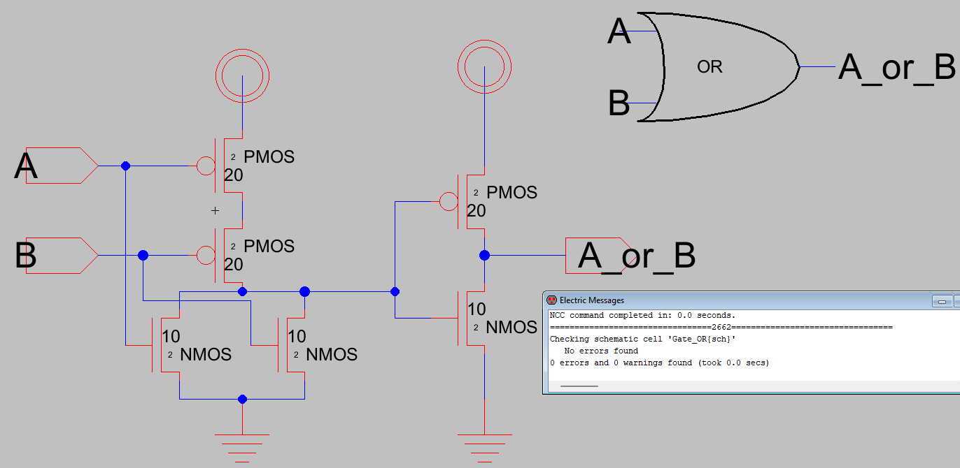
Figure 9: The OR Gate Schematic and Icon with No Errors.
Next, we want to run a quick simulation to make sure it works.
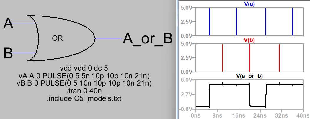
Figure 10: The OR Gate Simulation and Results.
Now, the layout of the OR Gate.
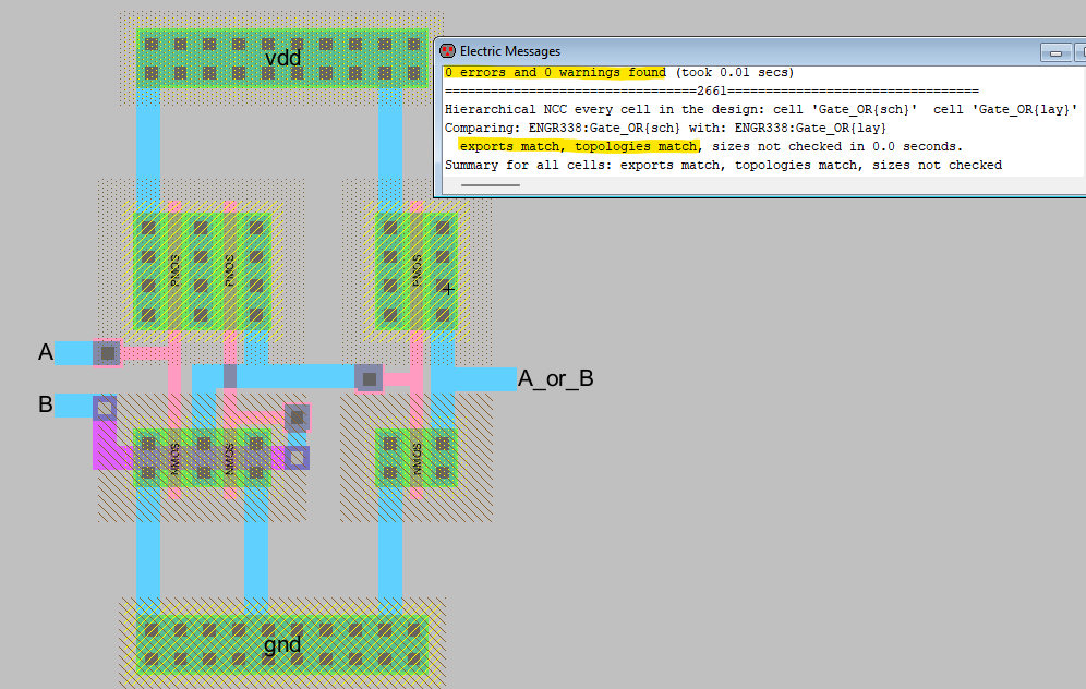
Figure 11: The OR Gate Created in Layout View with No Errors.
Now to tackle the 8-Bit OR Gate starting with the schematic and icon.
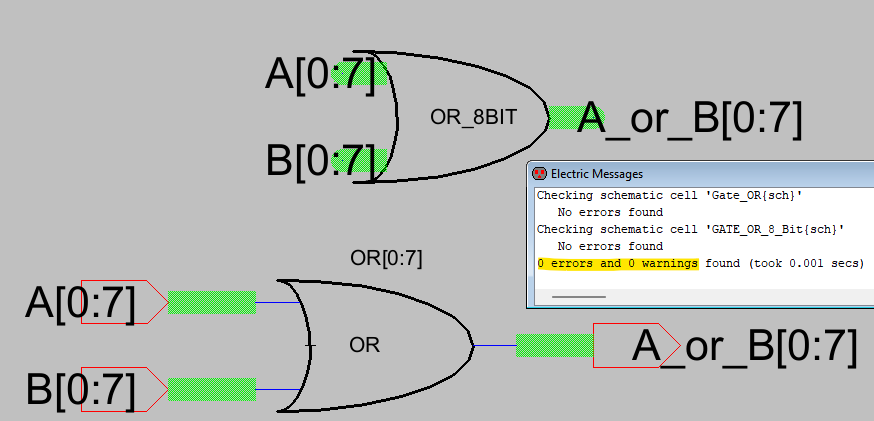
Figure 12: The 8-Bit AND Gate Schematic and Icon with No Errors.
Run a quick simulation to make sure it is working correctly.
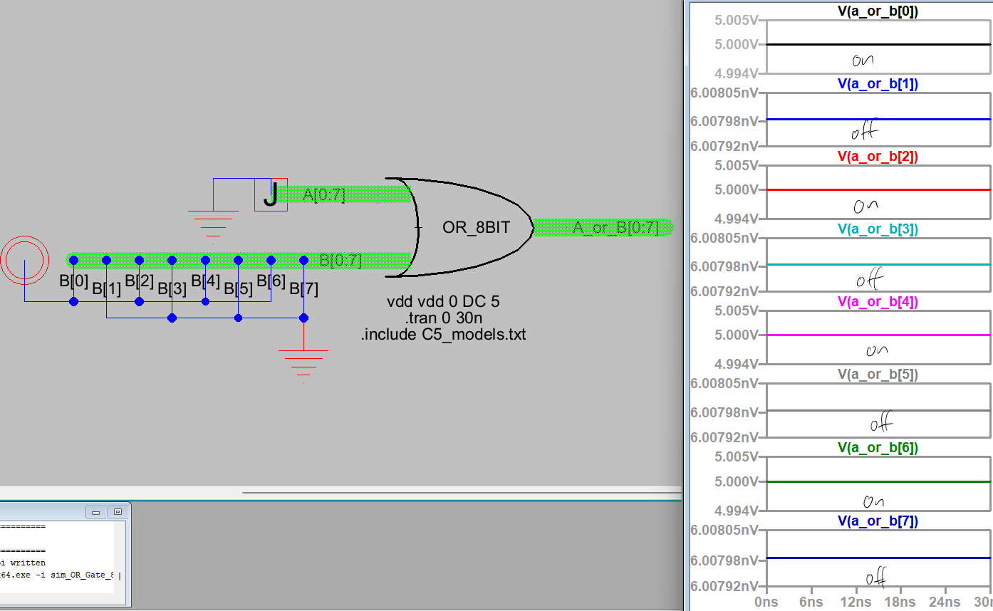
Figure 13: The 8-Bit OR Gate Simulation and Results.
Lastly, the layout.
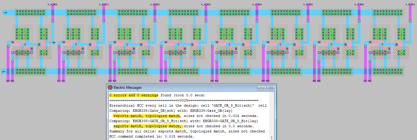
Figure 14: The 8-Bit OR Gate Layout with No Errors.
Task 4: Design an 8-bit NAND gate. (20 points)
First, we want to create the 8-Bit schematic and its icon.
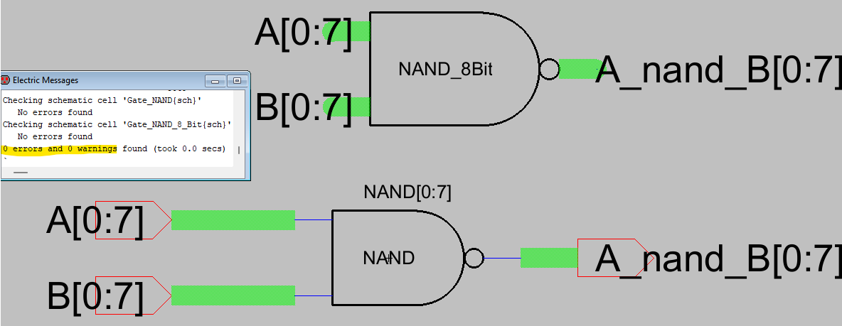
Figure 15: The 8-Bit NAND Gate Schematic and Icon with No Errors.
We'll run a quick sim to make sure it is working.
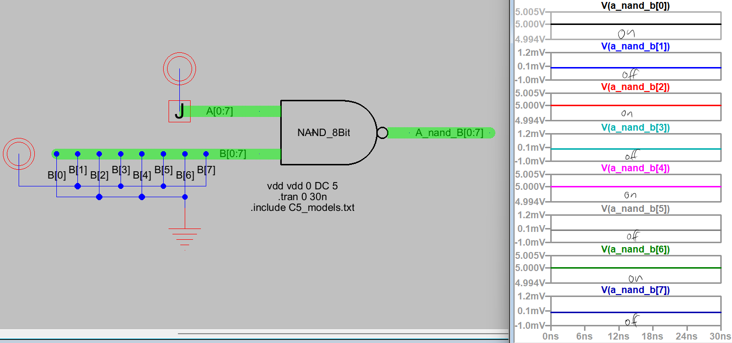
Figure 16: The 8-Bit NAND Gate Simulation and Results.
Now, the layout for the 8-Bit NAND gate.
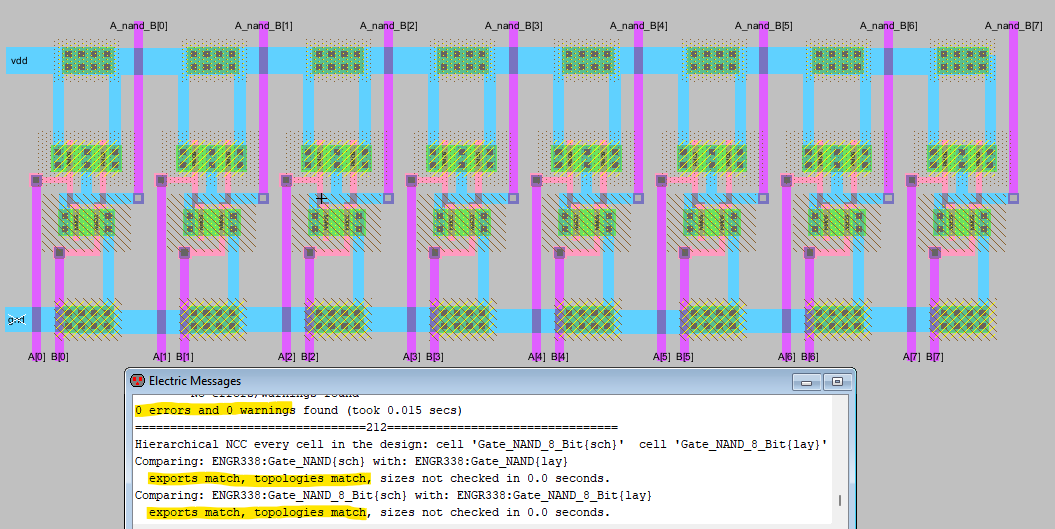
Figure 17: The 8-Bit NAND Gate Layout with No Errors.
Task 5: Design an 8-bit NOR gate. (10 points)
Now the 8-Bit NOR Gate.
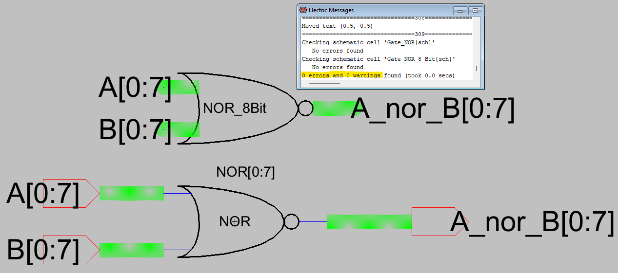
Figure 18: The 8-Bit NAND Gate Schematic and Icon with No Errors.
A quick simulation to make sure it is working correctly.
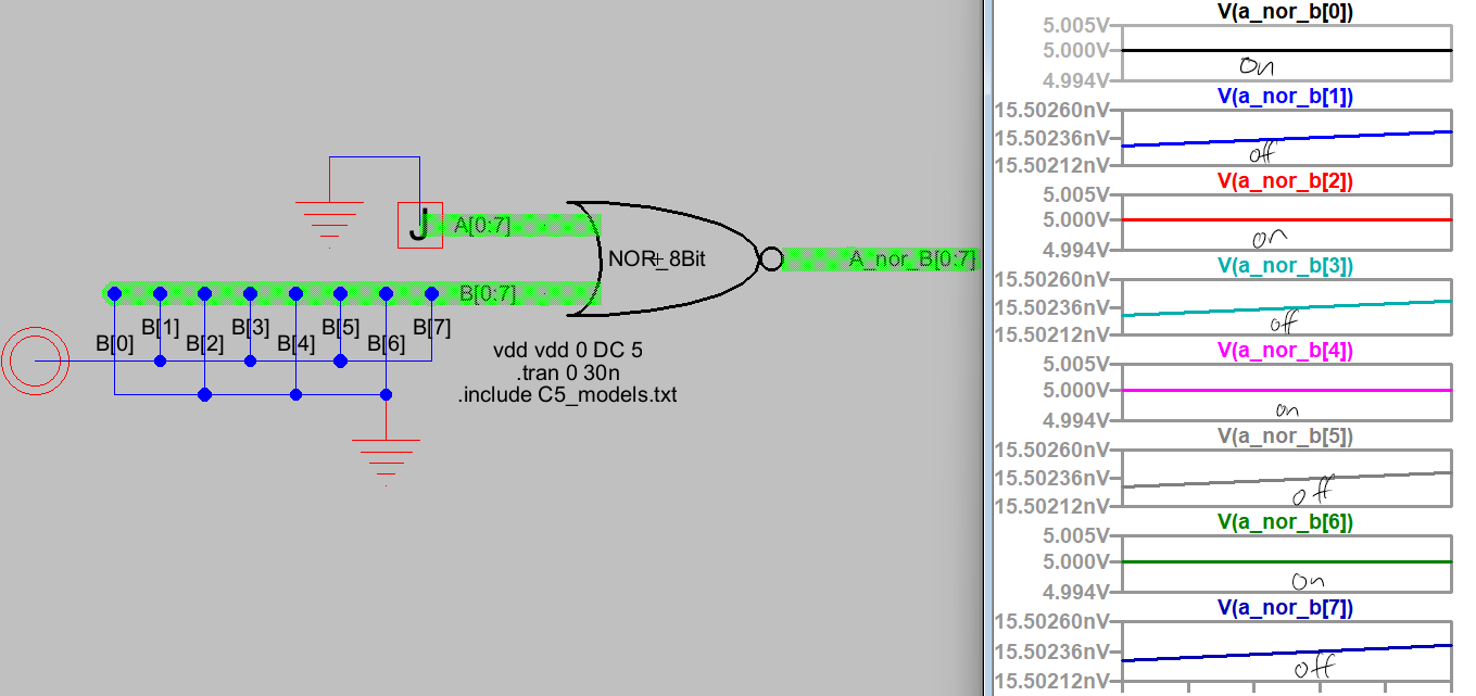
Figure 19: The 8-Bit NOR Gate Simulation and Results.
Lastly, we need to do the layout.
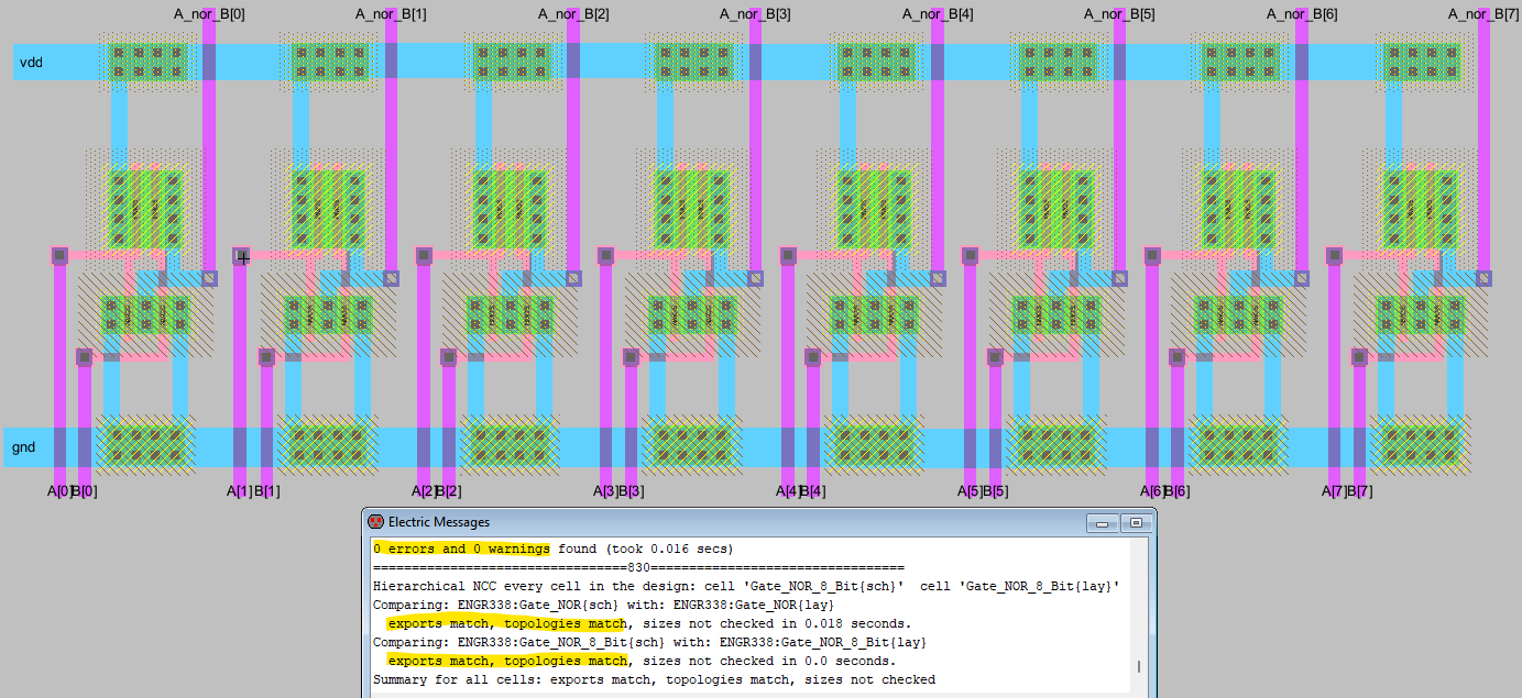
Figure 20: The 8-Bit NOR Gate Layout with No Errors.
Discussion
This lab was great. I feel more comfortable creating layouts in ElectricVLSI.