CE 338 Lab 2023 Fall
Lab 6: Build a NAND, NOR, XOR, and
Full Adder
Name: Vann Montoya
Email: bvmontoya@fortlewis.edu
Build
a NAND, NOR, XOR, and Full Adder
Introduction
The purpose of this lab is to build different components using Electric
VLSI.
Materials and Methods
Electric VLSI
Results
Task
1: Create the schematic and layout of the NAND gate. (15 points)
Here is the simulation of the nand gate:
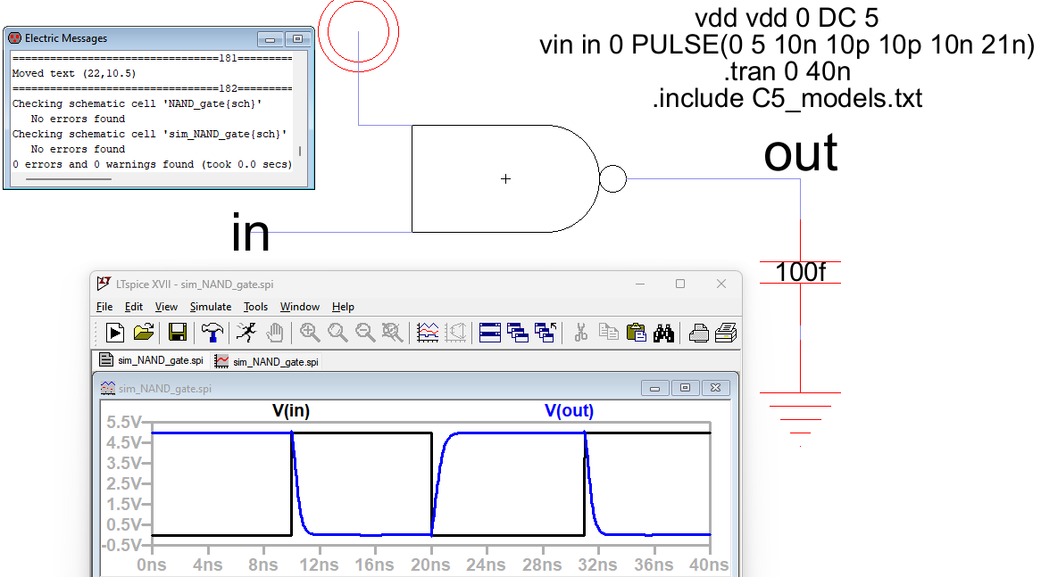
Figure 1: NAND gate icon, simulation and results.
Now, to create the layout for the NAND gate.

Figure 2: Layout of the NAND gate with no errors.
Task 2: Create
the schematic and layout of the NOR gate. (15
points)
Here is the simulation of the NOR gate.
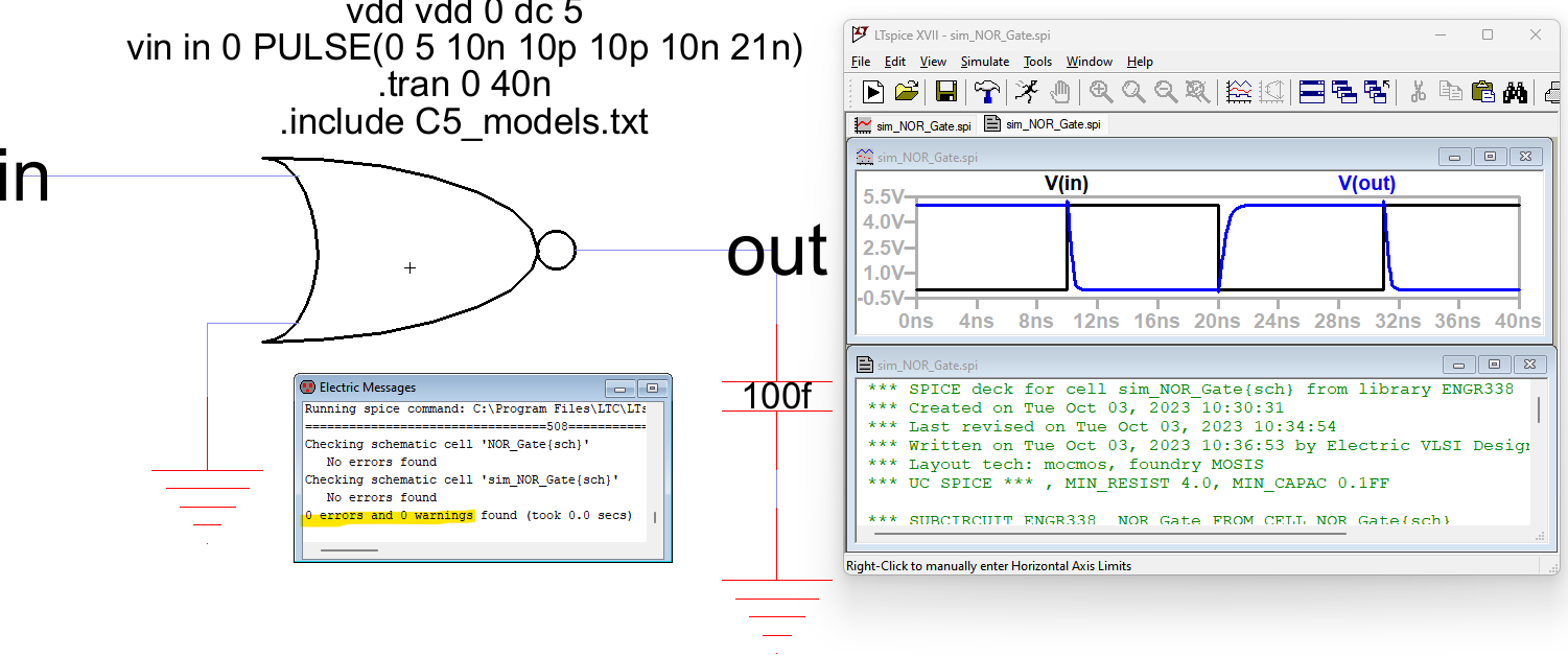
Figure 3: NOR gate icon, simulation and results.
Now, to create the layout of the NOR gate.

Figure 4: Layout of the NOR gate with no errors.
Task 3: Design, simulte, and
layout an XOR gate. (30 points)
Here is the simulation of the XOR Gate.
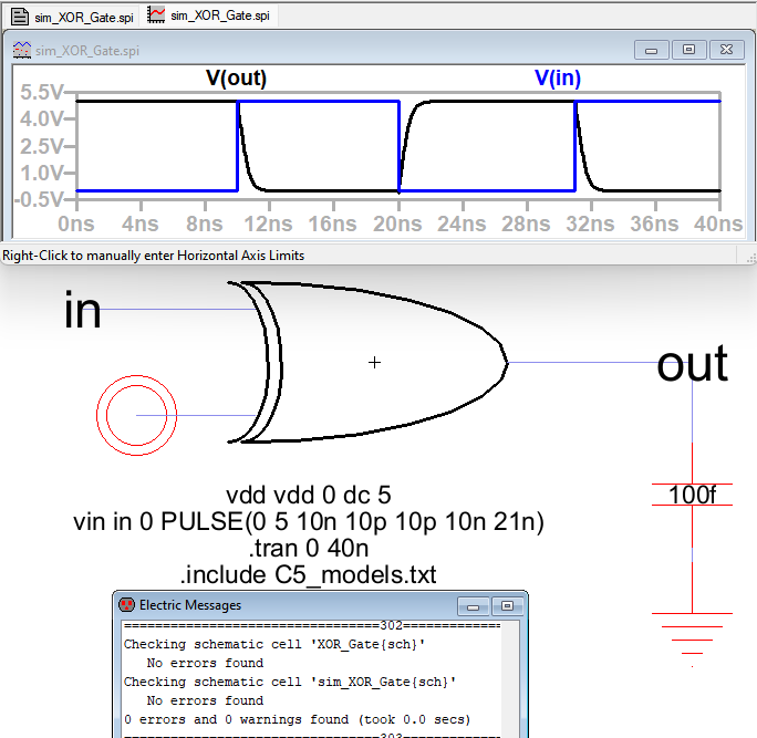
Figure 5: XOR gate icon, simulation and results.
Now to create the layout for the XOR gate.
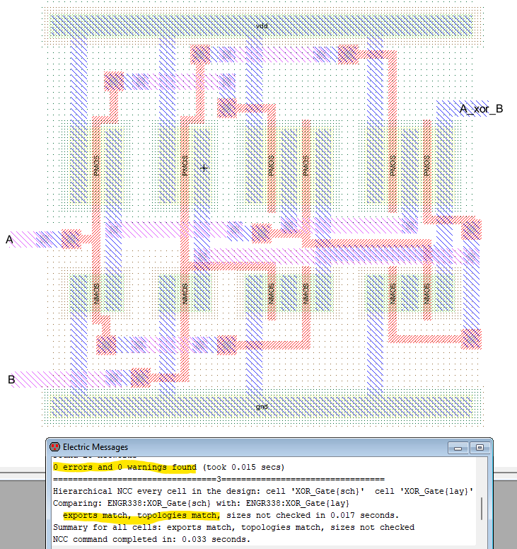
Figure 6: Layout of the XOR gate with no errors.
Task 4: Design, simulte, and
layout an Full Adder. (30 points)
Here is the schematic of the Full Adder created using logic gates.
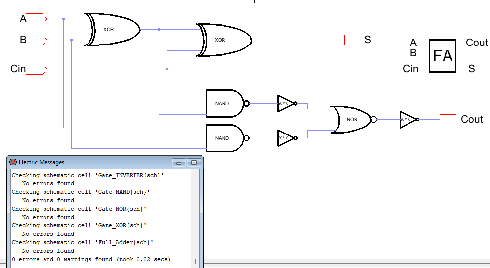
Figure 7: Schematic of the full adder using our premade logic gates and its symbol.
Now, we want to simulate the circuit.
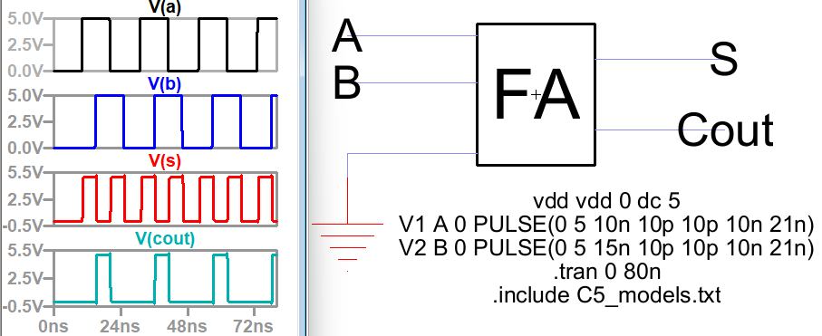
Figure 8: Full-adder icon, simulation and results.
Lastly, we want to create the layout.
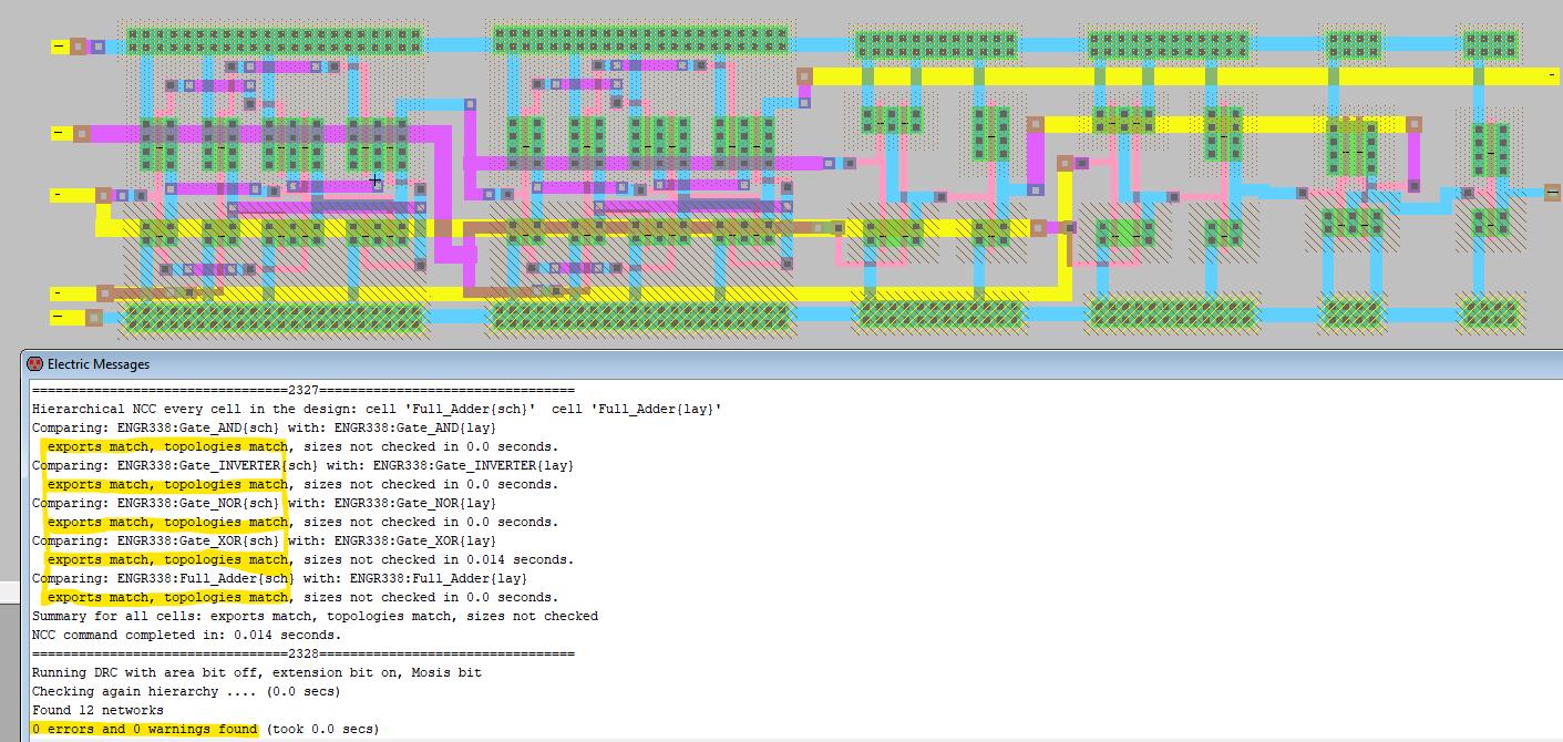
Figure 9: Layout of the Full Adder with no errors.
Discussion
This lab was a great way to practice using ElectricVLSI, however, the
layout view is very tedious to work with and hard to understand errors.