CE 338 Lab 2023 Fall
Lab 2 Design an R-2R DAC
Name: Vann Montoya
Email: bvmontoya@fortlewis.edu
Design an R-2R DAC.
Introduction
- The
purpose of this lab is to understand ideal ADC and DAC and become
familiar with Electrics VLSI and LTSpice for integrated circuit design.
Materials and Methods
- LTSpice
- Electric VLSI
Results
Task 1: Copy the existing ideal ADC-DAC files to your ENGR338 library and run the simulation. (30 points).
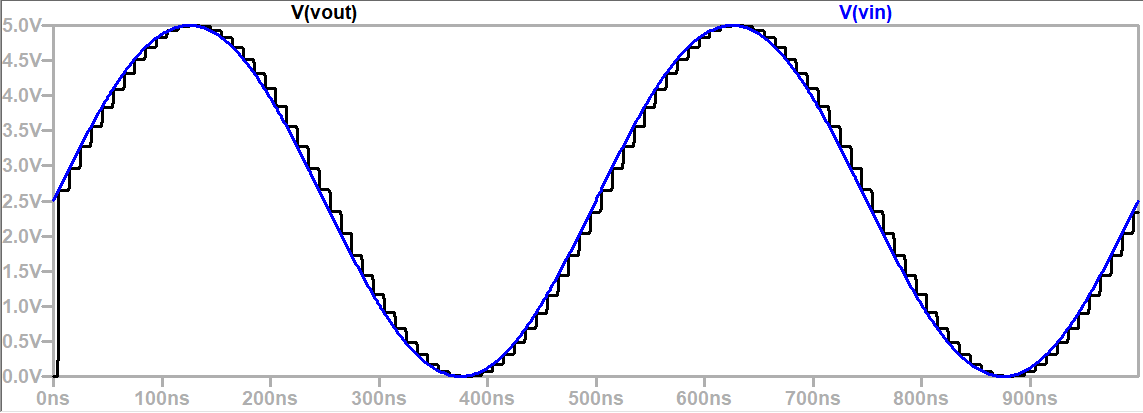
Figure 1: LTSpice simulation results for the ideal ADC-DAC setup.
Task 2: Build the schematic of the R-2R DAC and run the simulation. (30 points).
Here is the circuit schematic and its symbol as well as replacing the DAC in the original simulation.
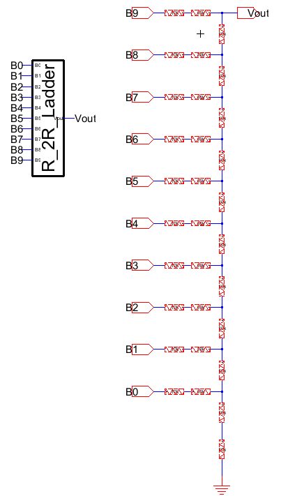
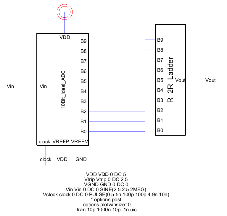
Figure 2: Circuit of the R 2R Ladder, its symbol, and how it is connected to the ADC.
Here is are the results from the simulation:
Figure 3: Simulation results from the replaced DAC.
Task 3: Test the time delay from the B9 pin when the DAC drives a 10 pF load. (30 points).
Here is the circuit schematic for only pin B9 connected and pins B8 - B0 grounded.
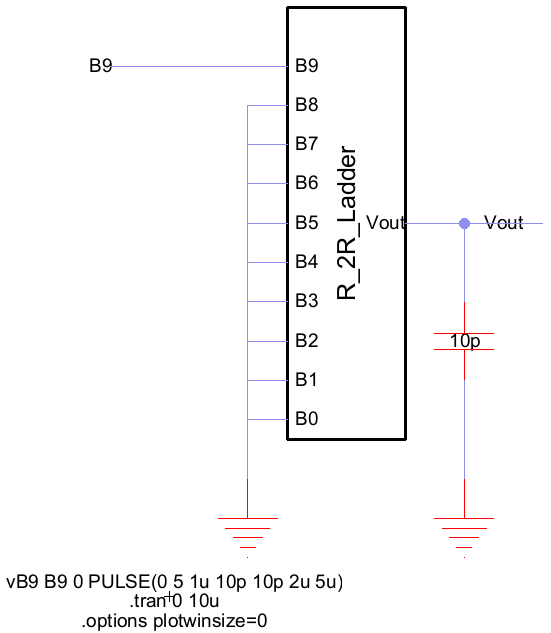
Figure 4: Circuit for Task 3.
Here's the results from the simulation:
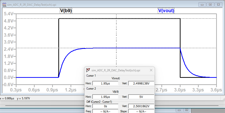
Figure 5: Results from task 3 simulation.
Discussion
This lab was a great way to introduce Electrics VLSI.