ENGR 338 Lab 2021 Fall
Course Project
Name: Brian Tsosie
Email: bjtsosie@fortlewis.edu
8-bit SAR ADC
Introduction
Building an SAR ADC in Electric VLSI.
Materials and Methods
Classmates
|
LT Spice software
|
Electric VLSI software
|
Results
1. Sample & Hold Circuit
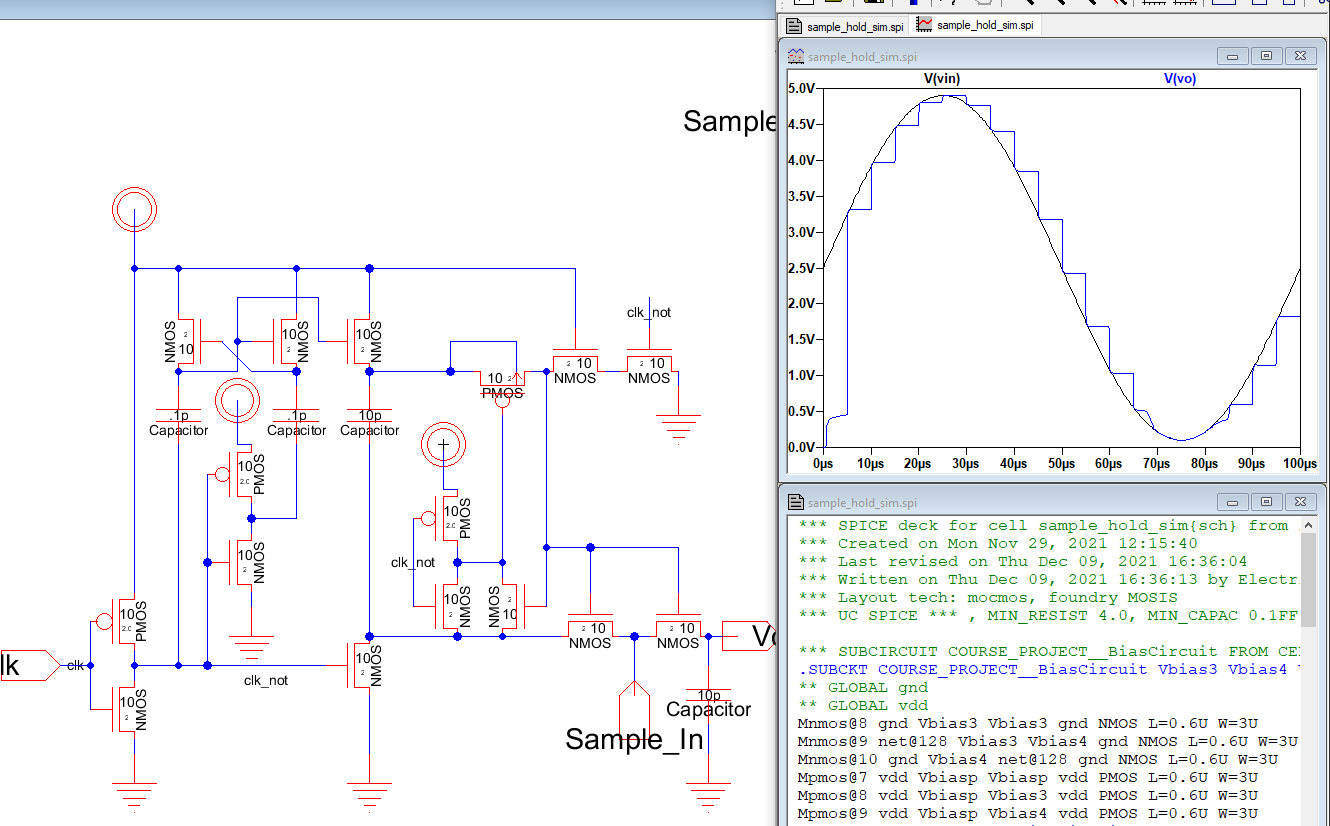
Figure 1. Sample and Hold schematic with LTspice simulation.
2. Operational Amplifier
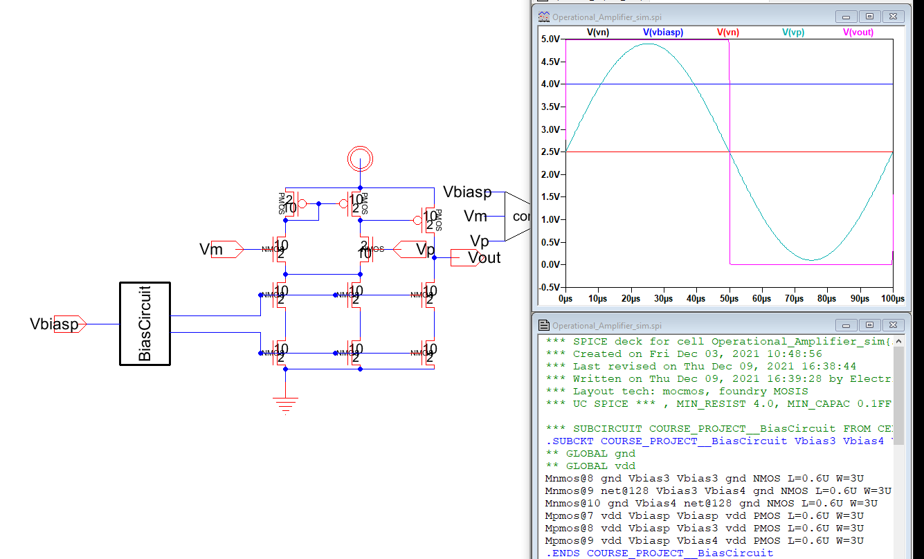
Figure 2. Opamp schematic with LTspice simulation.
3. SAR
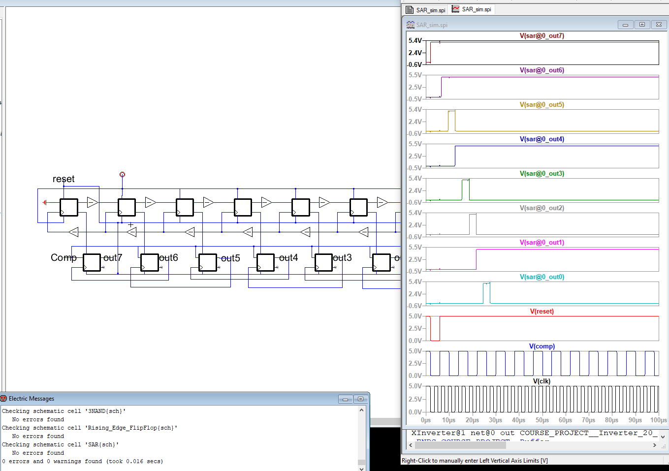
Figure 3. SAR schematic with LTspice simulation.
4. R2R DAC
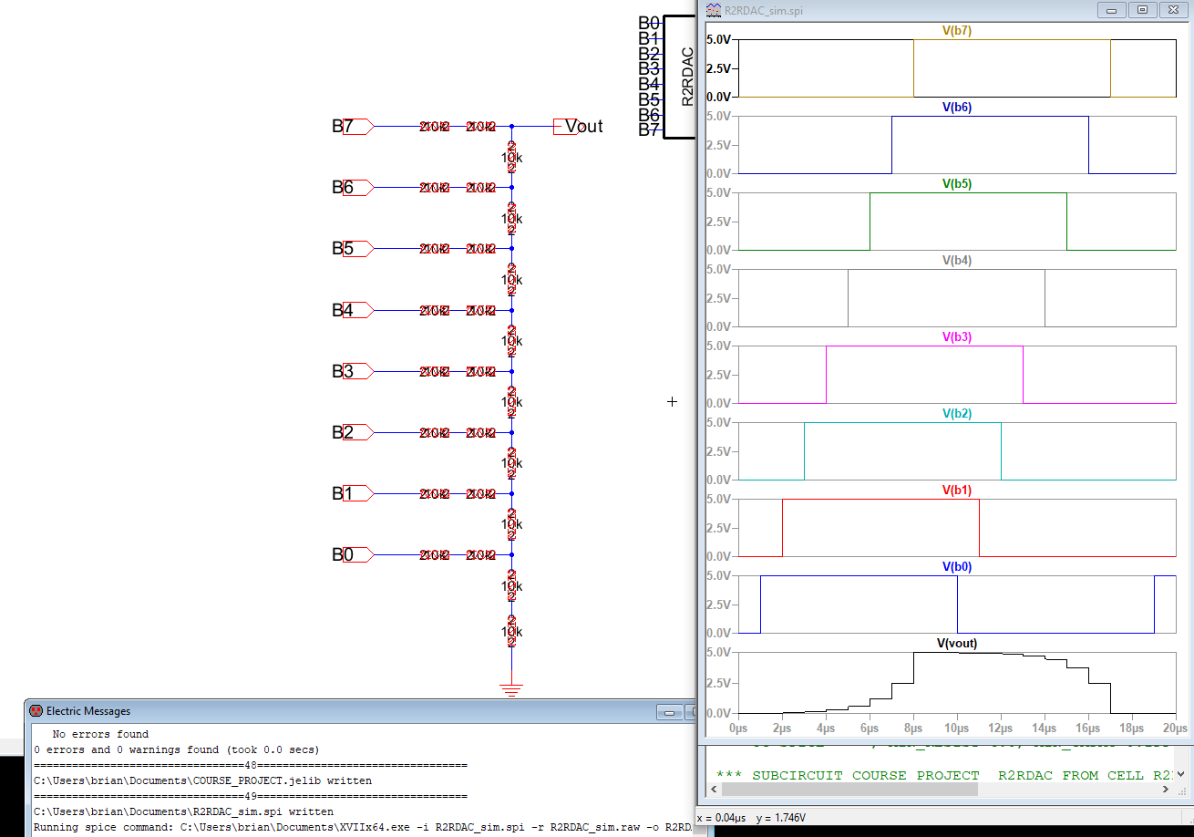
Figure 4. R2R DAC schematic with DRC and LTspice simulation.
5. Door Register
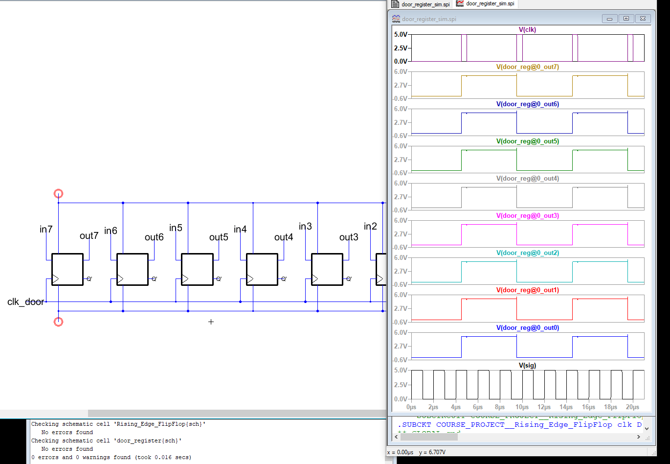
Figure 5. Door register with DRC and LTspice simulation.
6. Timming Block
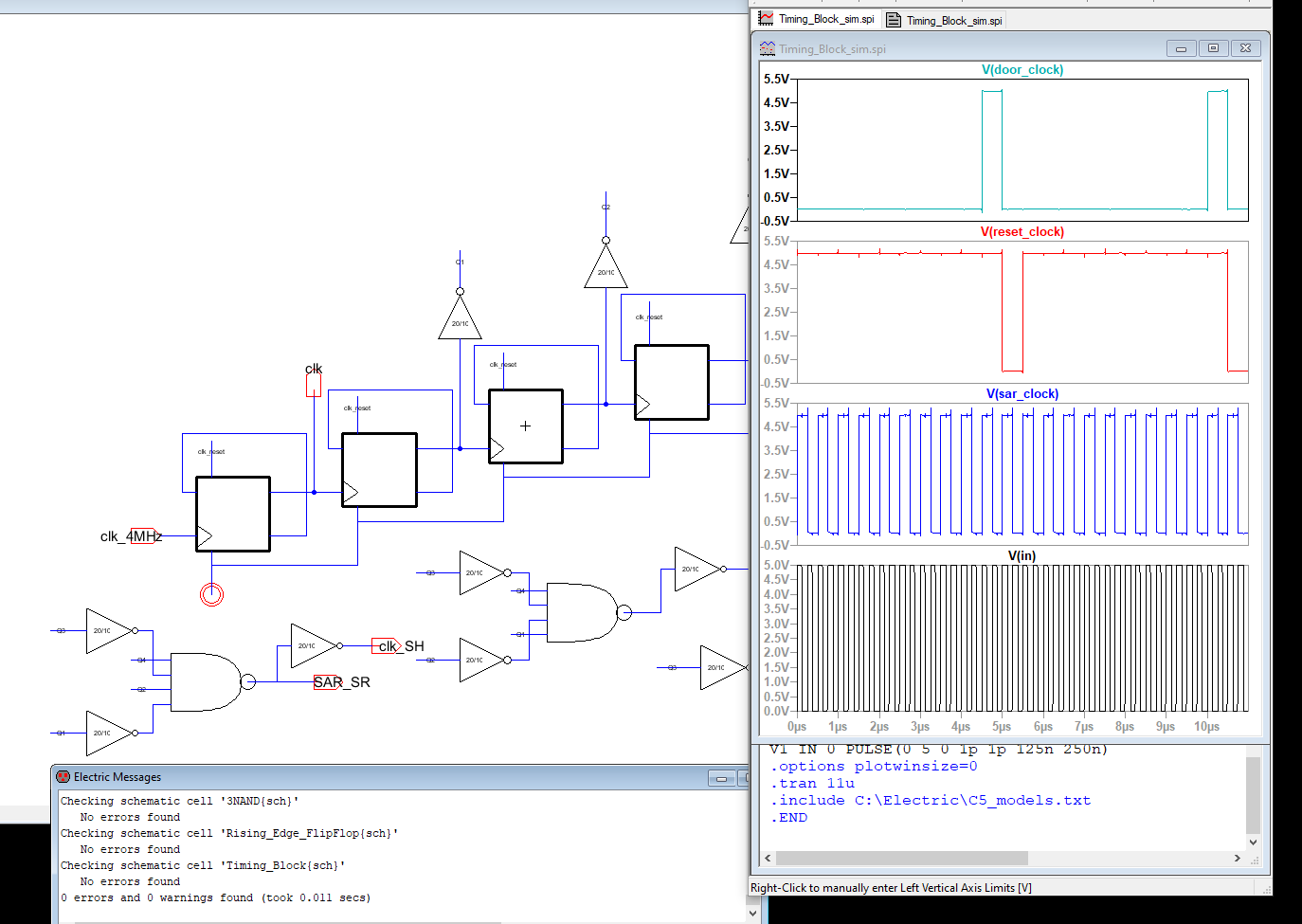
Figure 6. Timming block schematic with DRC and LTspice simulation.
7. SAR ADC
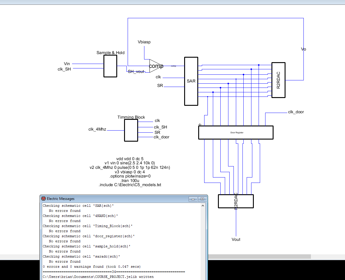
Figure 7. SAR ADC schematic with DRC.
8. SAR ADC
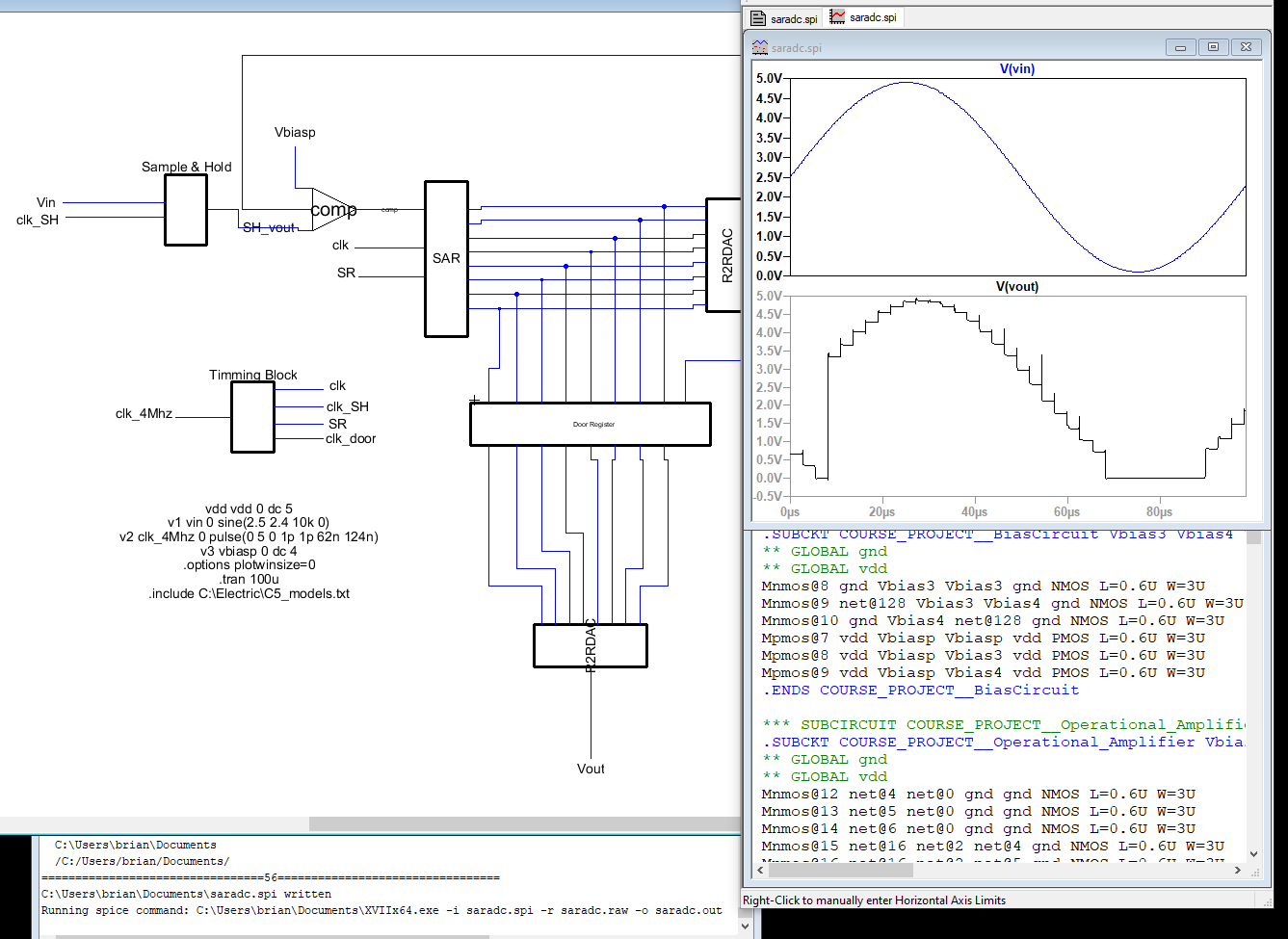
Figure 8. SAR ADC LTspice simulation.
Discussion
The building of the SAR ADC initially seemed straight forward. However,
it was easier said than done. The easiest circuit could be the R2R DAC.
All that was needed
was to modify the existing 10-bit circuit from lab 2. The other circuit
proved to be more challenging. So much so that the help of a fellow
classmate was needed. They
were able to give helpful advice and get me back on track. The SAR ADC
seems to be working more or less. I'm sure there are things that could
be done to make
it work better. This final lab was rather difficult for me. Without any
help, this overall circuit may not have worked as well or not at all.