ENGR 338 Lab 2021 Fall
Lab 9
Name: Brian Tsosie
Email: bjtsosie@fortlewis.edu
Simple 8-Bit ALU
Introduction
Building an 8-bit ALU.
Materials and Methods
Pencil & Paper
|
LT Spice software
|
Electric VLSI software
|
Results
Task 1: Logic circuit of the ALU.
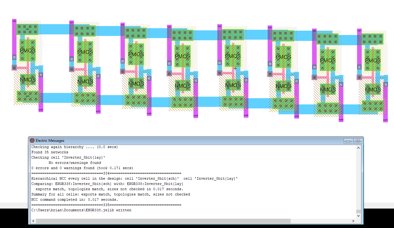
Figure 1. Layout of an 8-bit inverter with DRC and NCC.
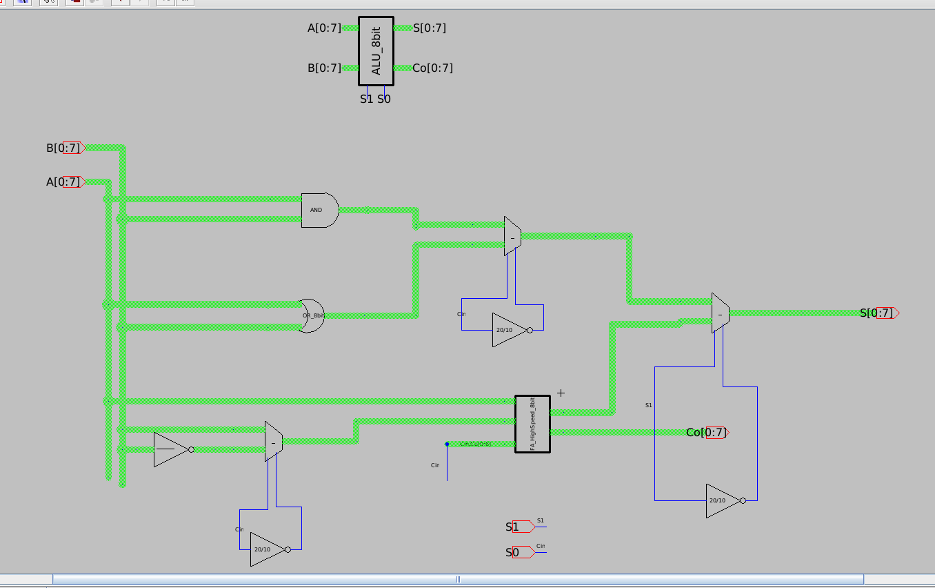
Figure 2. Schematic of the 8-bit ALU.
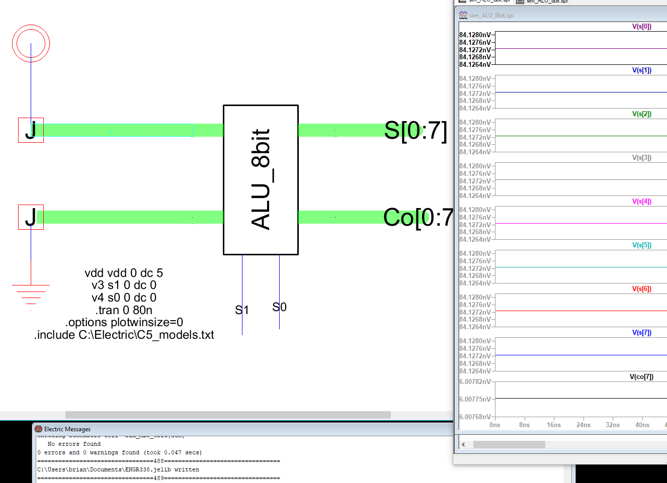
Figure 3. Simulation to verify AND gate by setting S1S0=00.
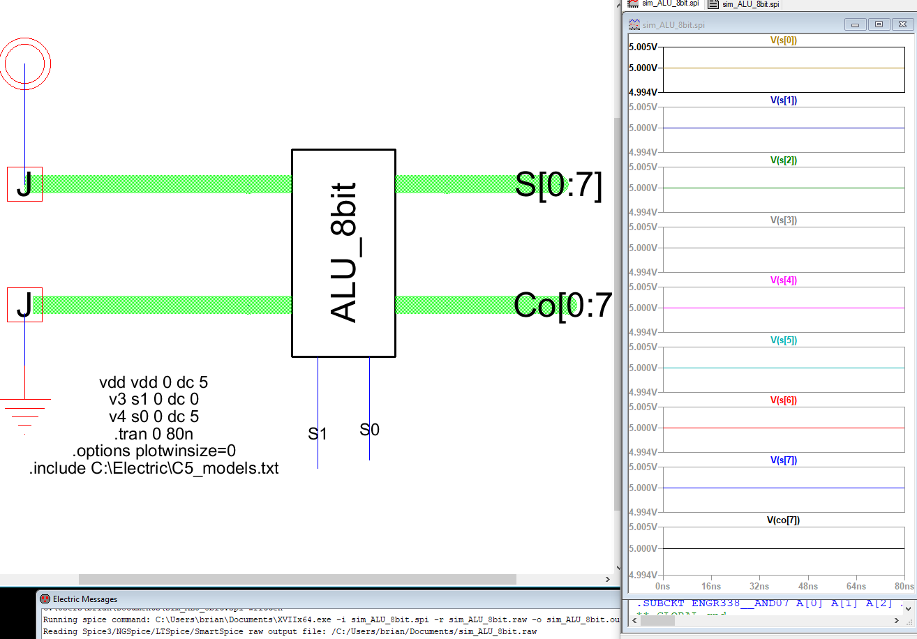
Figure 4. Simulation to verify OR gate by setting S1S0=01.
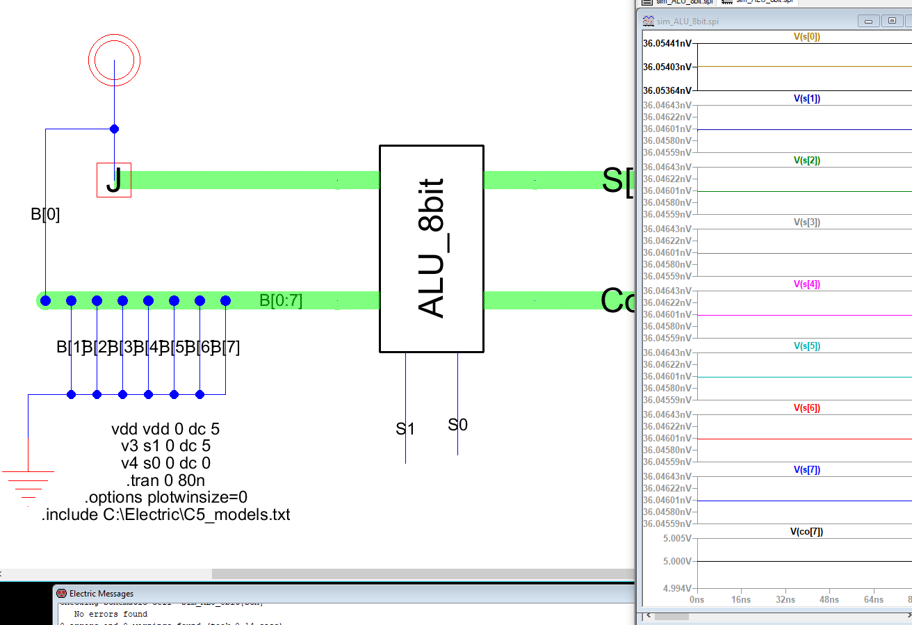
Figure 5. Simulation verifying AND operation using 1111 1111 + 0000 0001 = S = 0000 0000, Co=1.
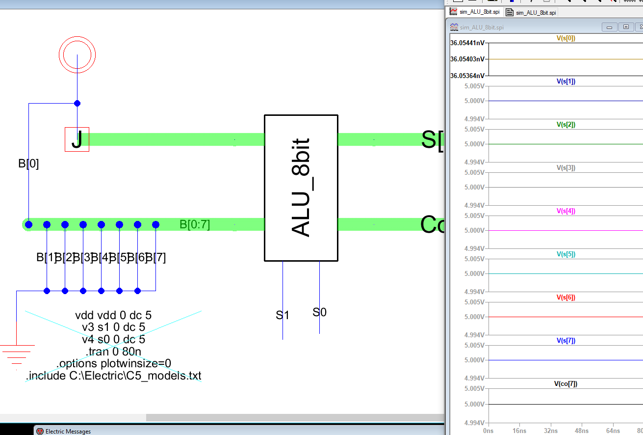
Figure 6. Simulation to verify the subtraction operation.
Task 2: ALU layout.
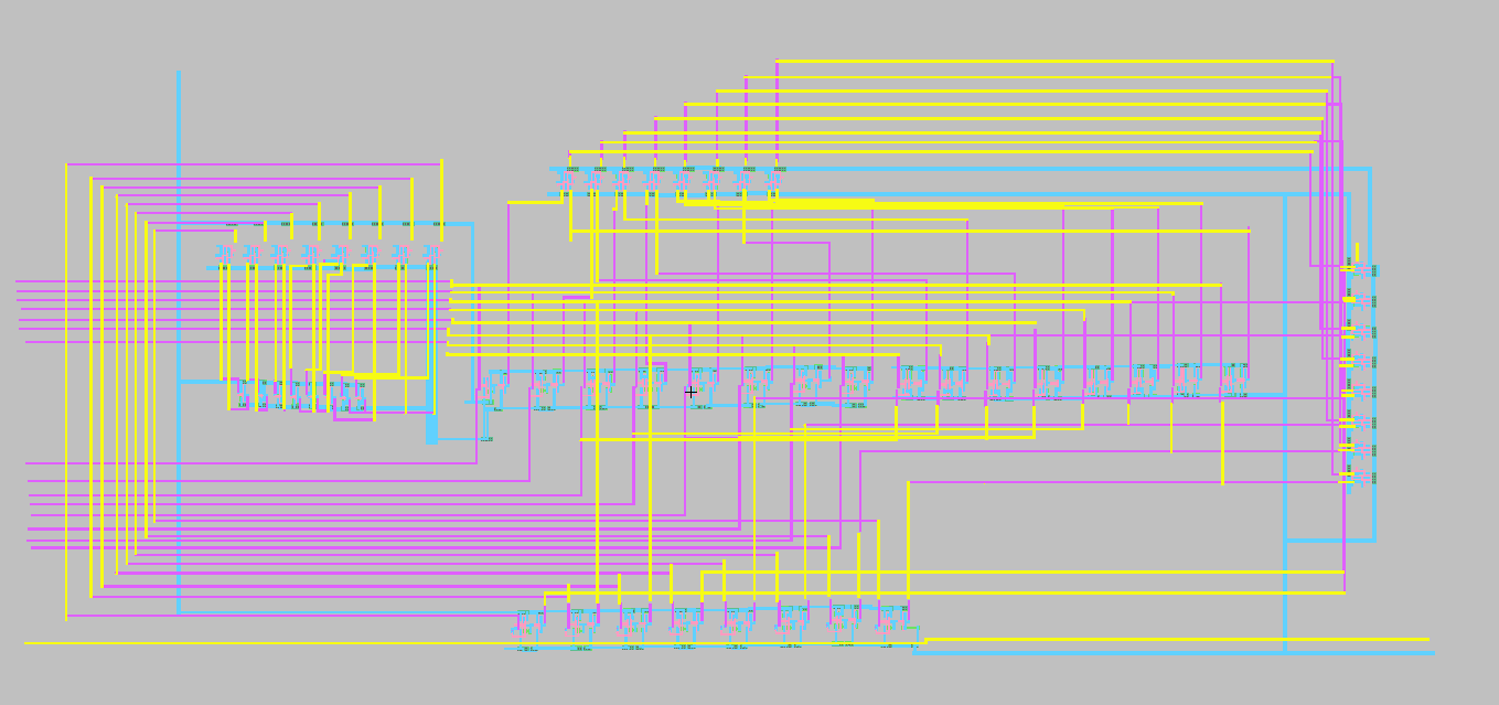
Figure 7. 8-bit ALU layout.
Discussion
Building the ALU layout proved to be very challenging. While the
layout could be considered straight forward, connecting all the
components together was not an easy task.
So much that the DRC and a NCC checks did not pass. It was easy to get
lost and lose track of what went where and spacing each component just
right. Unfortunately, that
is what happen here.