ENGR 338 Lab 2021 Fall
Lab 6
Name: Brian Tsosie
Email: bjtsosie@fortlewis.edu
Building a NAND, NOR, XOR and Full Adder
Introduction
Building NAND, NOR, XOR gates and combining the to build a Full Adder
Materials and Methods
Pencil & Paper
|
LT Spice software
|
Electric VLSI software
|
Results
Task 1: NAND gate
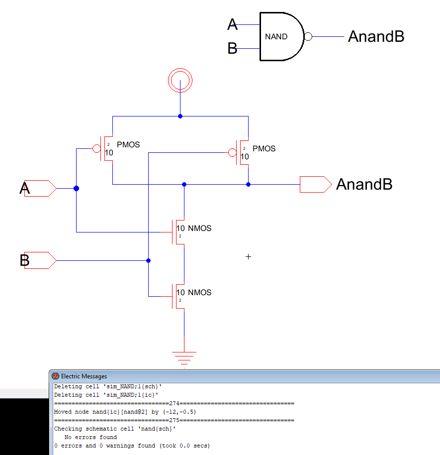
Figure 1. Schematic of a NAND gate and icon.
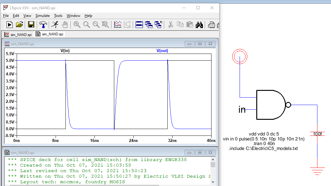
Figure 2. NAND gate simulation.
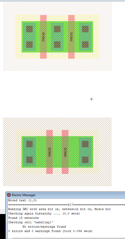
Figure 3. Initial NAND gate layout with DRC.
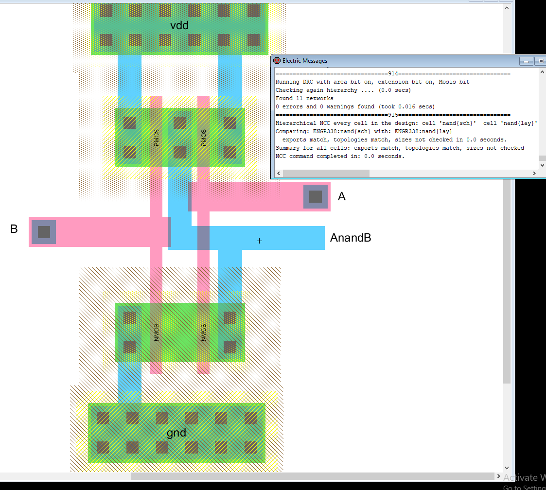
Figure 4. Final NAND gate layout with DRC.
Task 2: NOR gate
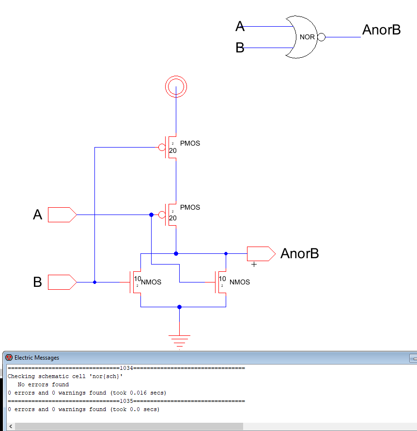
Figure 5. Schematic of NOR gate with DRC.
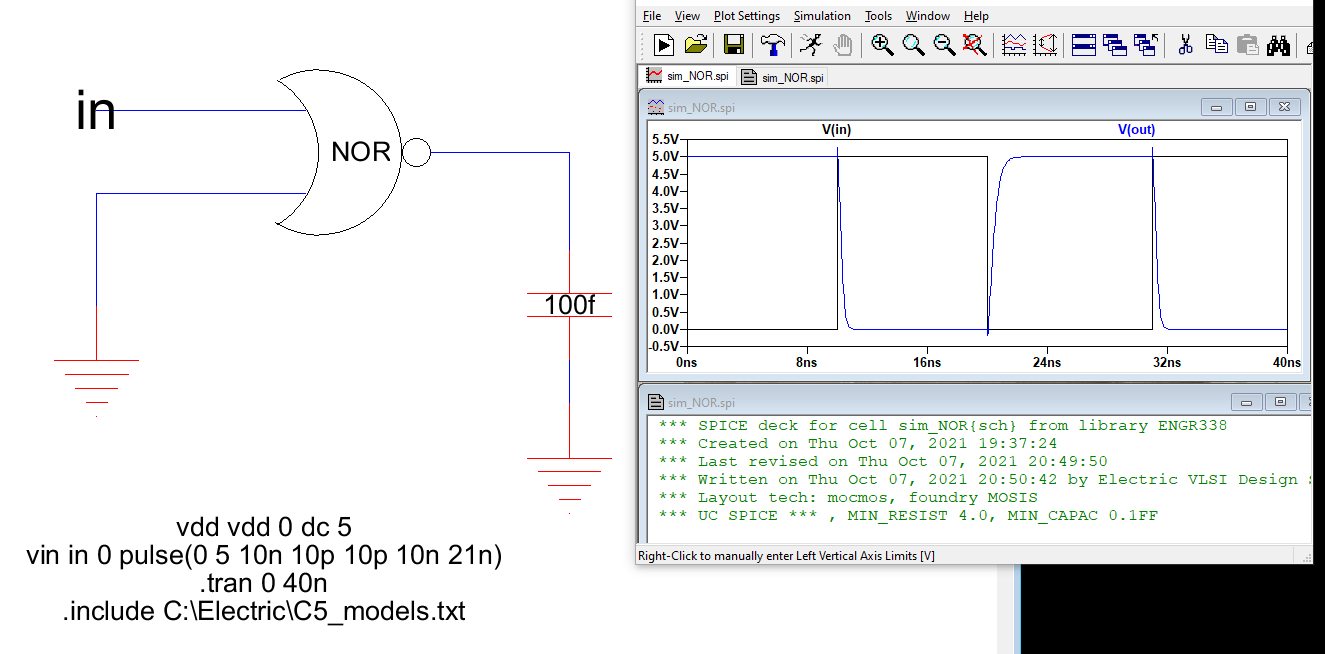
Figure 6. NOR gat simulation.
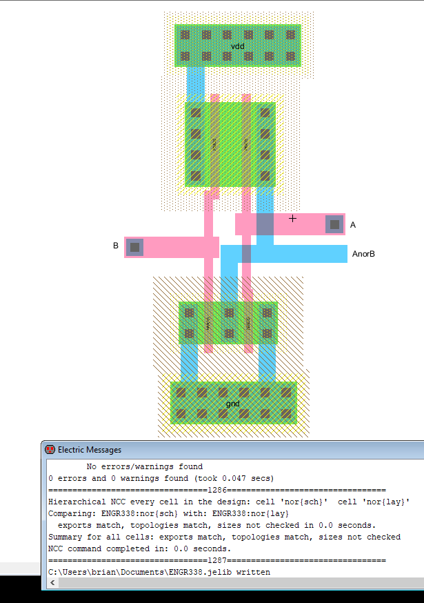
Figure 7. NOR gate layout with DRC.
Task 3: XOR gate
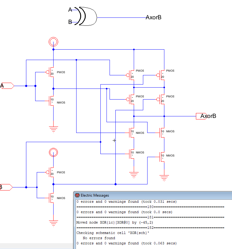
Figure 8. XOR schematic with DRC.
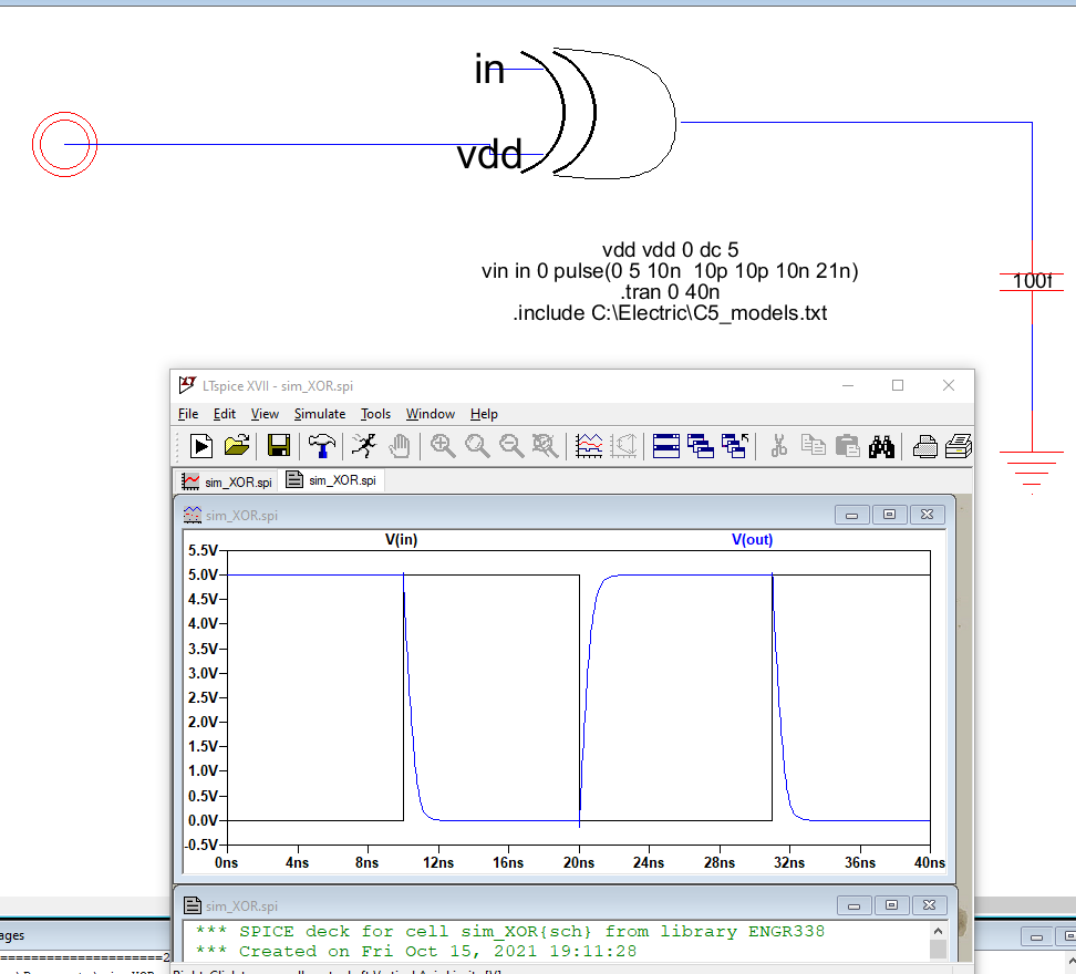
Figure 9. XOR simulation with 100 fF capacitor.
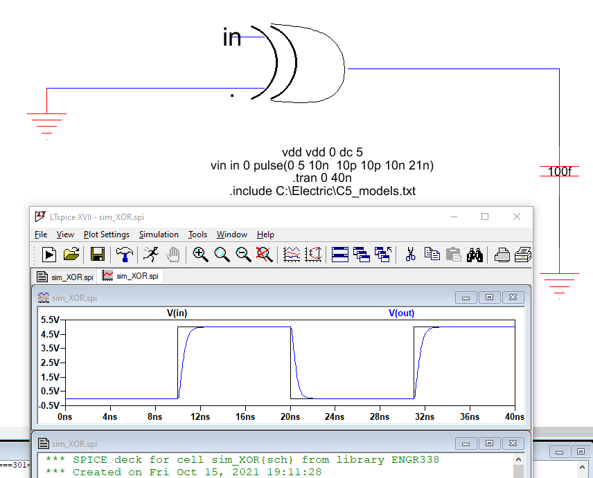
Figure 10. XOR simulation with grounded input and 100 fF capacitor.
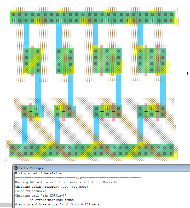
Figure 11. XOR layout with DRC.
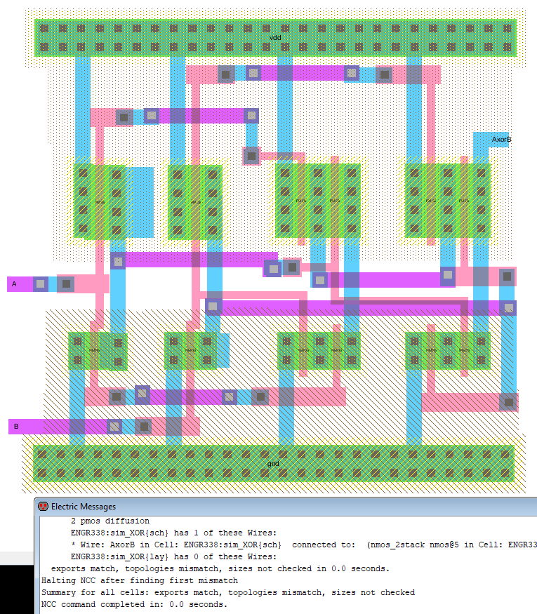
Figure 12. XOR layout with NCC.
Task 4: Full Adder
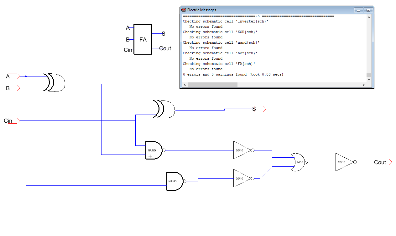
Figure 13. Full Adder schematic with DRC.
Discussion
Three gates were constructed and a full adder. The three gates were
used to build the full adder. NAND, NOR, and XOR simulations went as
planned. However,
the XOR layout didn't match up with the schematic. There seemed
to be an extra wire somewhere in the layout or a missing wire somewhere
in the shematic.
The mismatch could not be located and rebuilding the layout was not a
viable option. While the NAND, NOR, and XOR gate got simulated,
combining them all
together to make the full adder and trying to get an output was not successful.