CE 433 2023 spring
HW5
Name: Anders Burdick-Levang
Email:
aaburdicklevang@fortlewis.edu
HW #5
1.
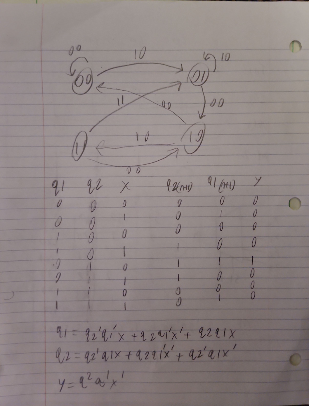
In Section 1, don't look at the logic equations provided to you. From
the state table, find the logic equations for q1(n+1) and y and draw
the sequential circuit for q1(n+1) and y.

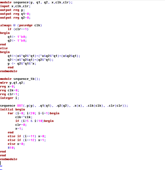
2. Repeat the work in Section 3. Use two methods, the given one and the behavioral one. Show simulation results.
3.
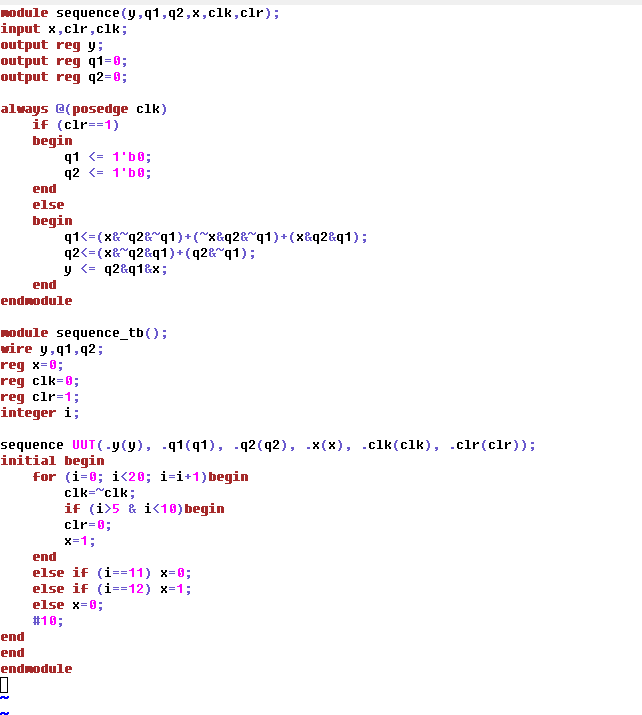
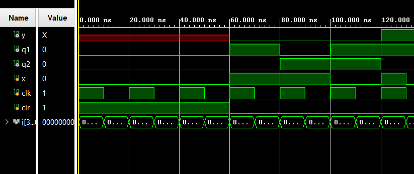
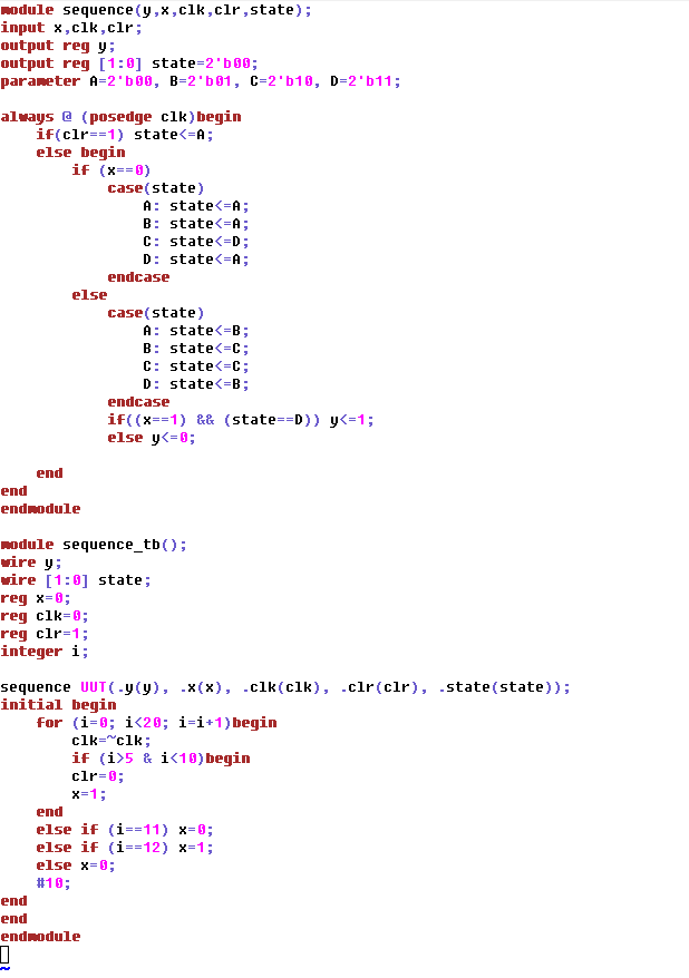
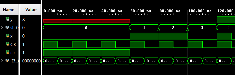
Similar to the sequence detector in Section 3, change the sequence to
be detected to 1011, design the state diagram, draw the truth table,
find the logic equations, and design the verilog module and testbench
to verify the logic.

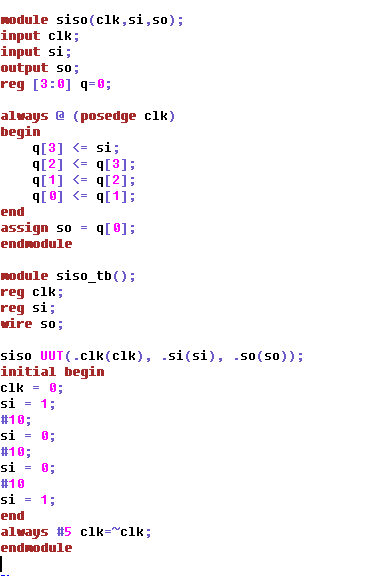
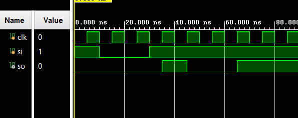
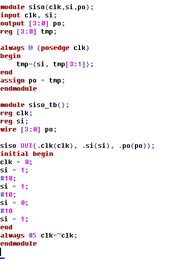
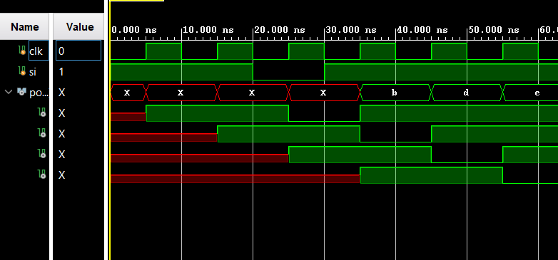
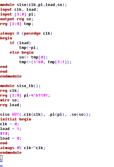
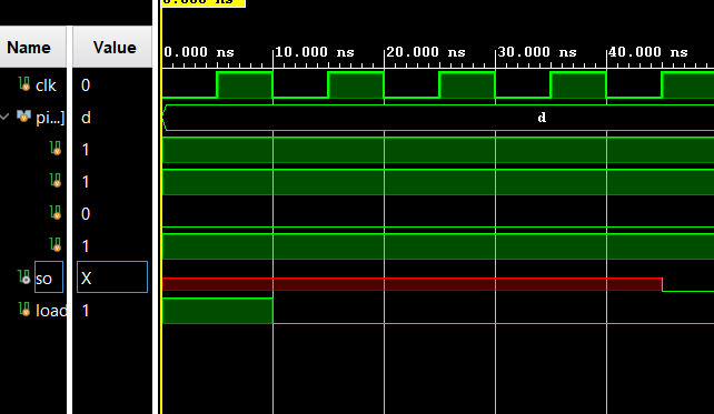
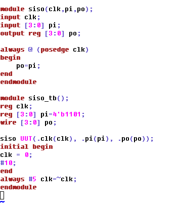
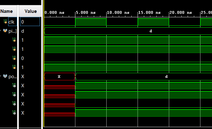
4. Simulate the four types of shift registers in Section 5.
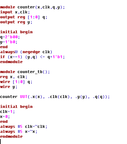
5. Build a counter module and show the simulation results.

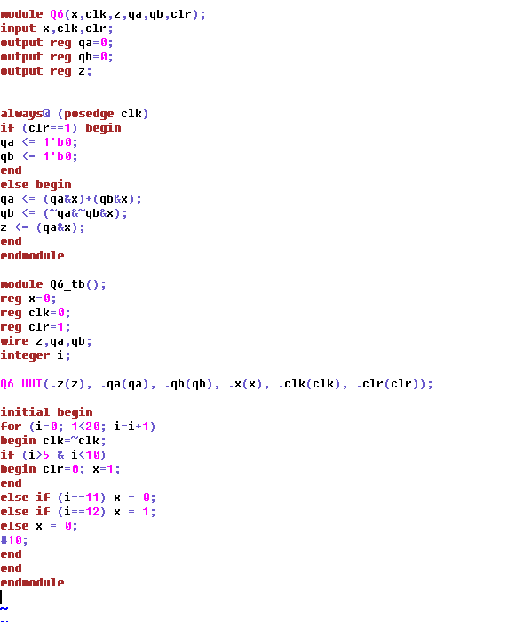
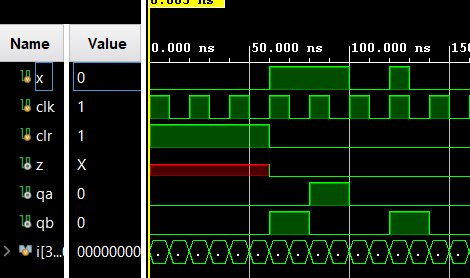
6. Find the logic equation of the following circuit and implement it in verilog. Show the simulation results.