CE338 Course Project (updated)
Since
the Cadence tutorials took longer to complete than I expected, we
should focus on a smaller module of the SAR ADC instead of rushing. For
the course project, we will build TI’s DFF circuit and run simulations
on it using the TSMC180 PDK.
You
have worked on this circuit in HW4 and HW5. We covered the timing and
logic of this circuit in the 2/24 and 2/26 lectures. Recorded videos
and notes are available on my website.
The
difference and the challenge here is to build and test it in Cadence
Virtuoso using the TSMC 180nm PDK. I don’t have a tutorial for this, so
you’ll need to explore and construct it using the skills you’ve
developed from Tutorials 1 through 7.
Here is the circuit schematic
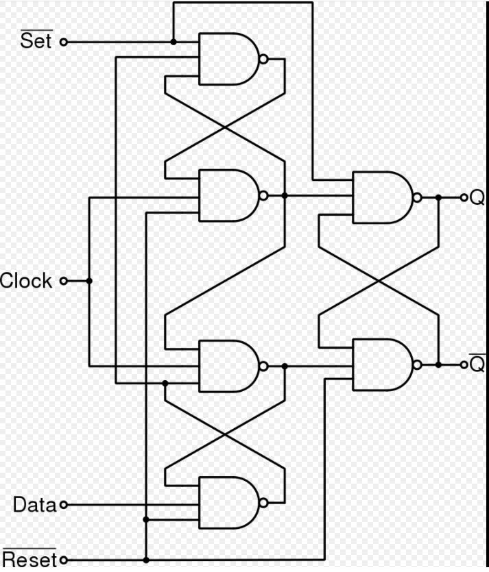
Step 1: Schematic Design (30 points)
1. Create the schematic and symbols of the 3-input NAND gates (15 points)
2. Build the TI DFF in another schematic, create a symbol out of it. It could be just a box with inputs/outputs (15 points)
Step 2: TI DFF symbol simulation (40 points)
You must create a new schematic and call it 'sim_NAND' for this task.
1. At the rising edge of the clock, data is sent to Q, Q_not is the inverse of Q. (10 points)
2. When clock is high, when data changes, Q and Q_not remain the same. (10 points)
3. When clock is low, changes to data do not change Q and Q_not. (10 points)
4. Set and Reset work as desired. (10 points)
Step 3: Create the layout (30 points)
1. Create the layout of 3-input NAND gates. DRC and LVS clean (15 points)
2. Create the layout of the TI DFF. DRC and LVS clean (15 points)