ENGR338 Digital Electronics Laboratory
Lab 7 Using Buses in ElectricVLSI
Objectives:
1. Be able to build a ring oscillator use buses.
2. Be able to build multi-bit gates in ElectricVLSI.
Lab Tasks:
Task 1:
Build and simulate a Ring oscillator. (20 points)
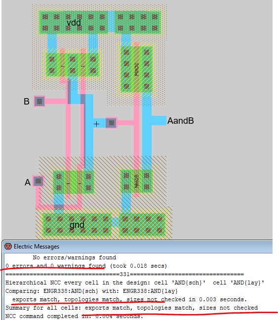
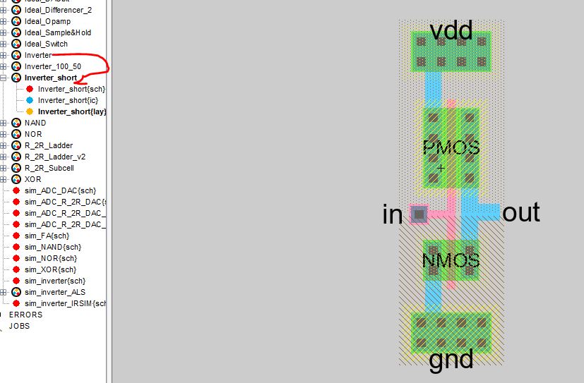
Duplicate
the tall inverter cell you created in Lab 4, rename it as
'Inverter_short'. Move the vdd/gnd rails closer to the MOSFETs. Then
run DRC/NCC before moving forward.
![](img/f1.jpg)
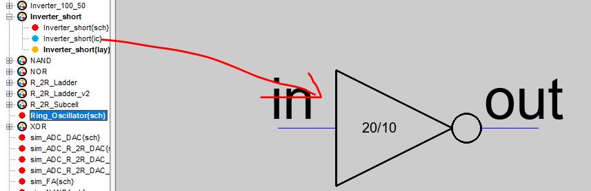
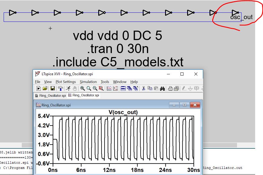
Create a new schematic view 'Ring_Oscillator'. Drag 'Inverter_short'
icon to the view.
![](img/f2.jpg)
Select the icon by left clicking it and press 'F6' to open the Array
setup window. The number '-6' means the inverters are being set apart.
This setup creates 11 inverters in a row.
![](img/f3.jpg)
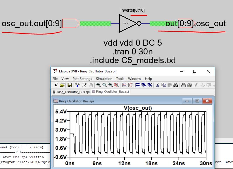
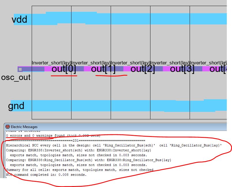
Connect them as a ring. I named the net at the very right hand side as
'osc_out' for LTSpice probing. You can pick up any node inside the ring
for display.
![](img/f4.jpg)
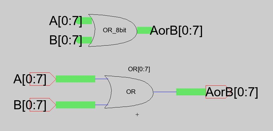
Next, let's build this in a different way (use data buses). Again,
create a new schematic view 'Ring_Oscillator_Bus'.
Select the inverter, press Ctrl + i to name it as 'inverter[0:10]'.
This will create 11 inverters in parallel virtually. It still shows a
single one in the view but there are 11 ones being created in the
netlist. [0], [1], [2], ...... [10].
Use the bus to connect the inverter to an input pin and an output pin.
Export the input pin as 'osc_out,out[0:9]' and the output pin as
'out[0:9],osc_out'.
![](img/f6.jpg)
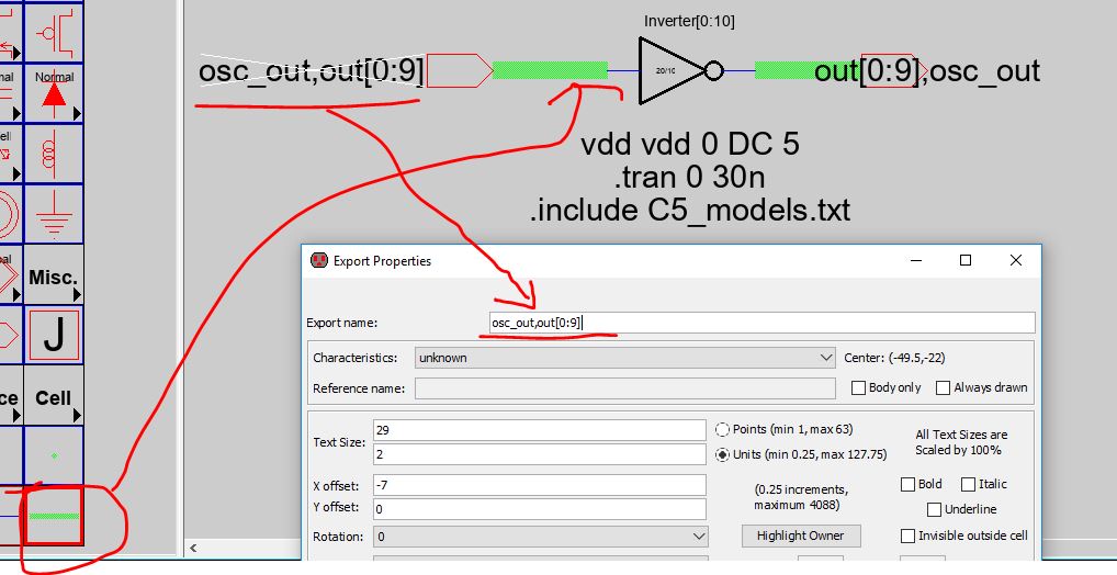
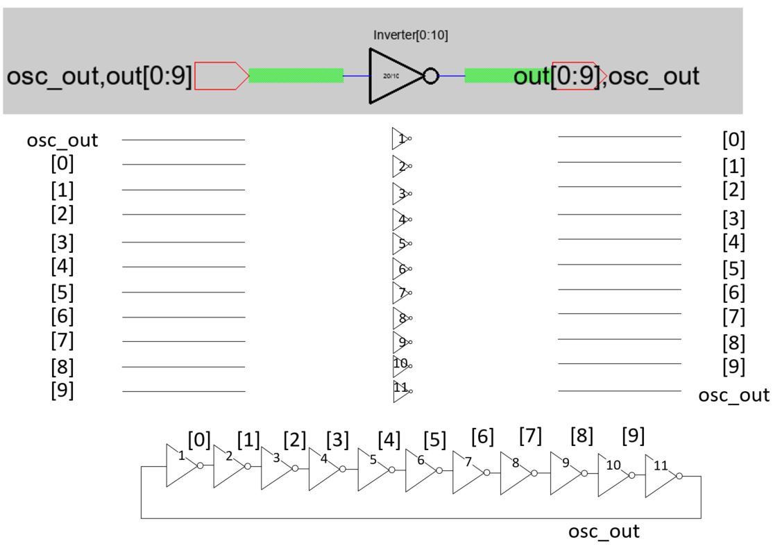
The input pin and the outpin are named as above is because in a ring
oscillator, the output of a inverter is shorted to the input of the
next inverter. The following diagram shows the input/output connections
of each inverter in this array.
![](img/f8.jpg)
If the schematic is DRC clean, use the same Spice code to run the
simulation. It shows the same results as the previous one.
![](img/f7.jpg)
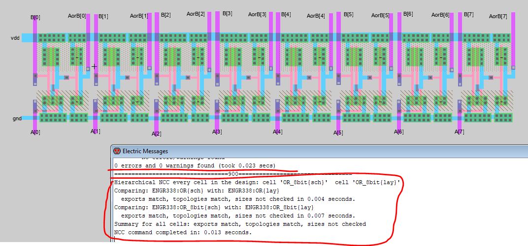
Next, the layout. Use buses is not an option in the layout view. Please
explain why in your report.
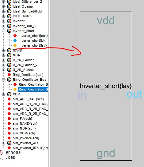
Drag the 'Inverter_Short' to the new layout view.
![](img/f9.jpg)
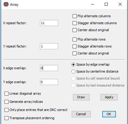
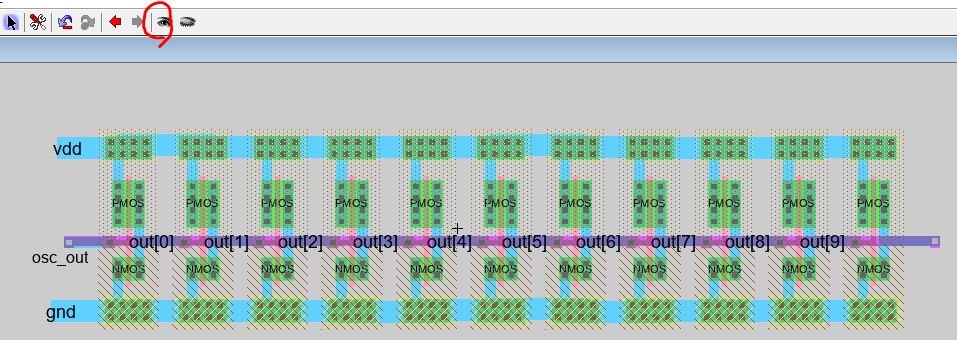
Make an array out of it.
![](img/f10.jpg)
Connect them in as a ring. Use Metal 1 to Metal 2 via at the left and
the right side of the row and then use Metal 2 to close the loop. DRC
it before you export the pins for LVS.
![](img/f11.jpg)
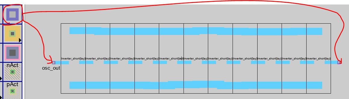
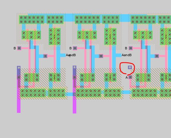
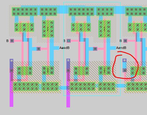
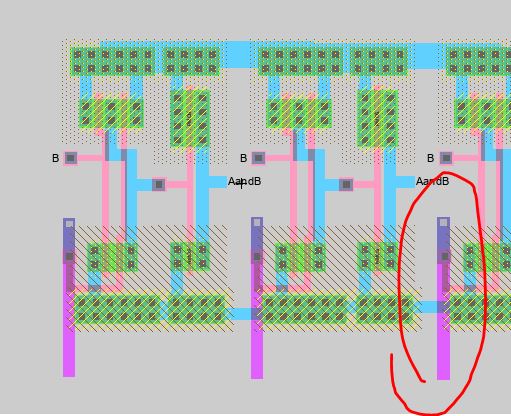
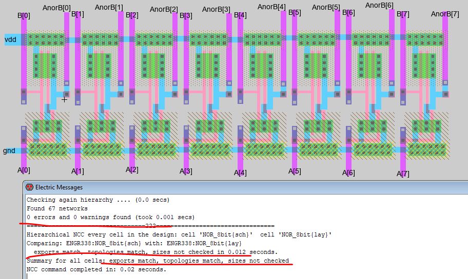
You must export all the 'out[0] - out[9]' ports to pass the LVS.
![](img/f12.jpg)
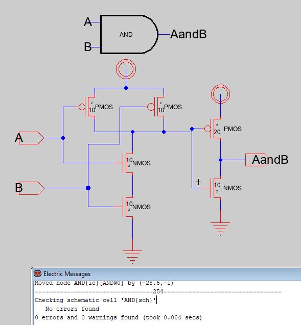
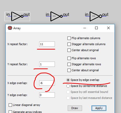
Show the internal circuit of the inverter:
![](img/f13.jpg)
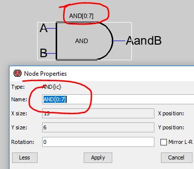
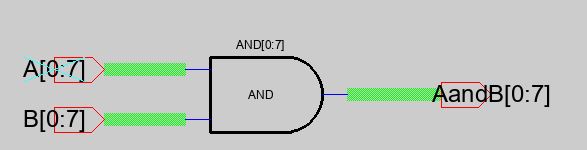
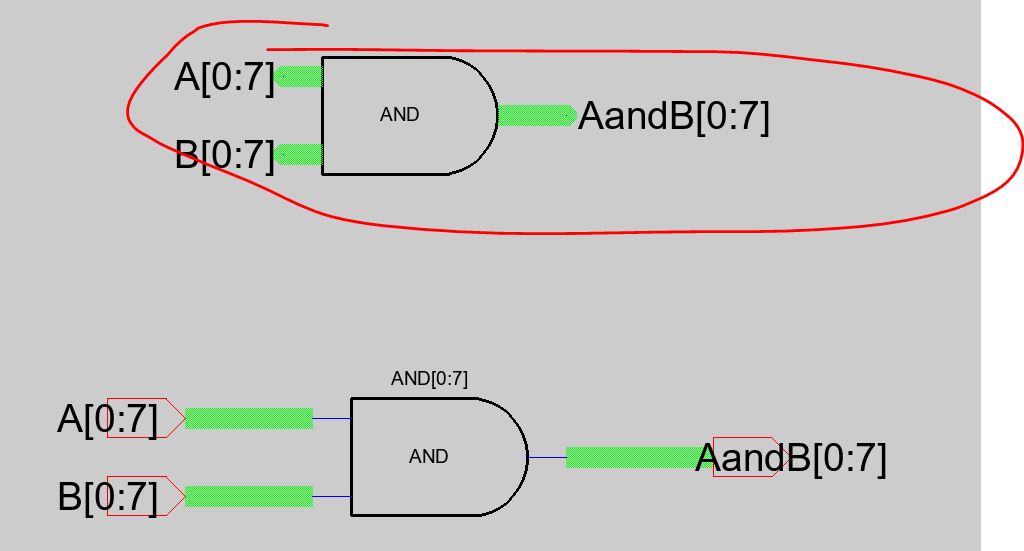
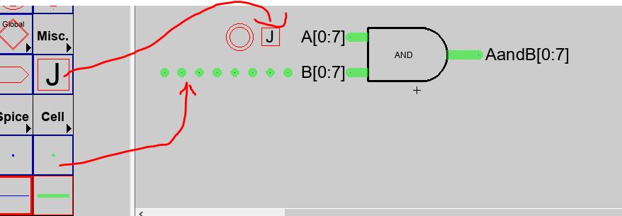
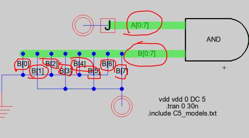
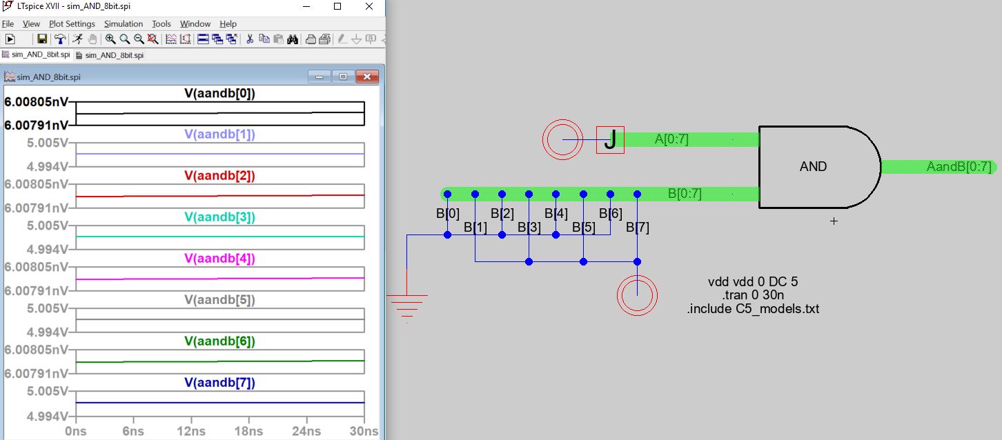
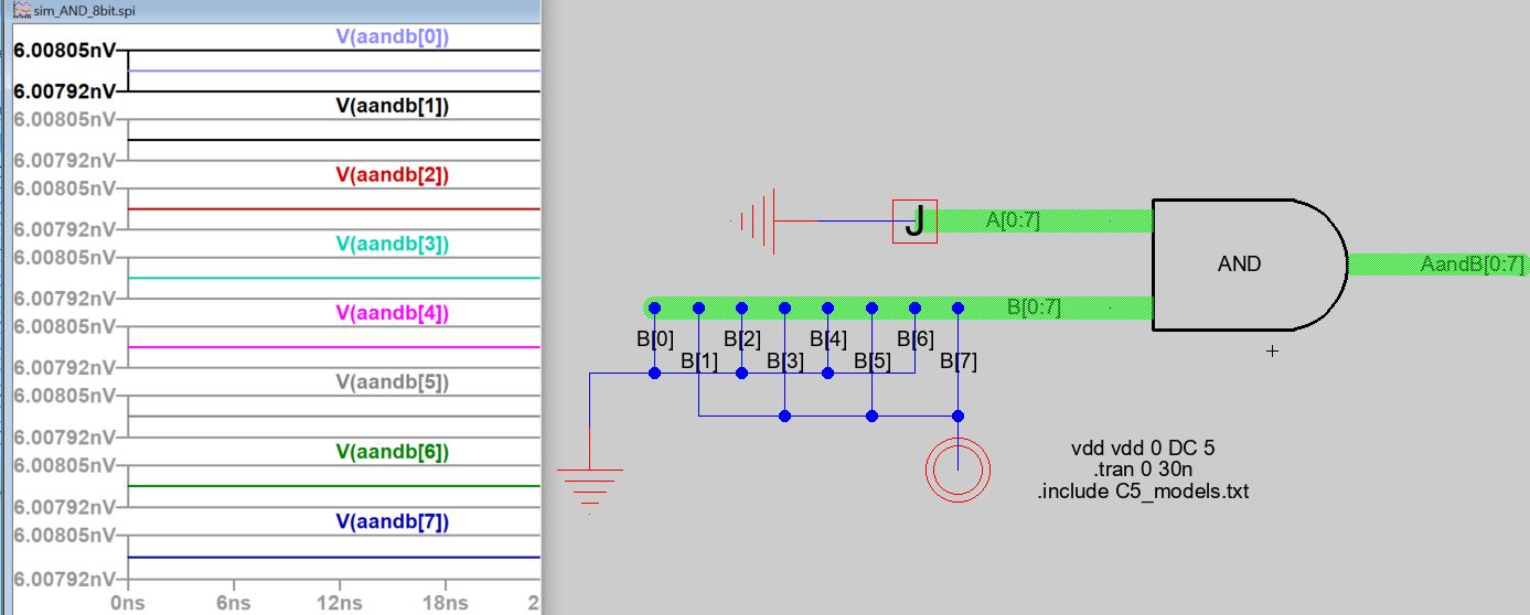
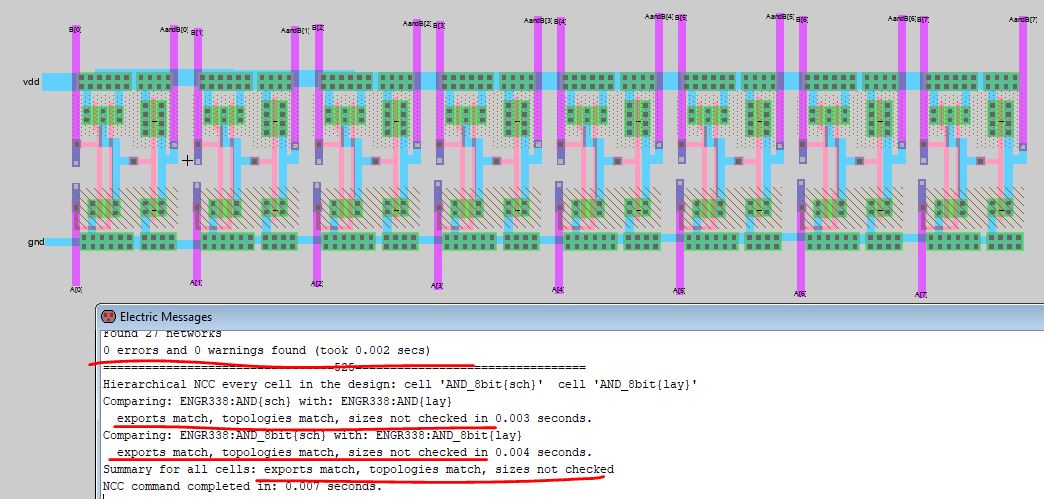
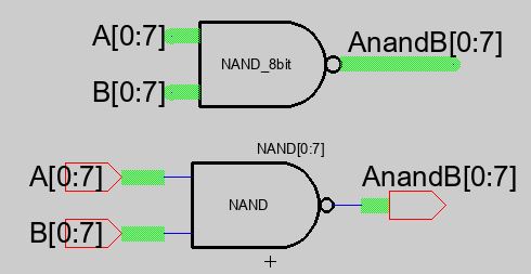
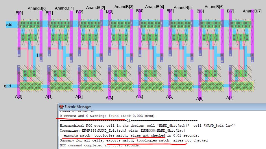
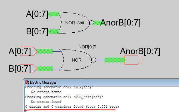
Task
2: Design an
8-bit AND gate. (20 points)
I re-used the parts of the schematic/icon of the NAND gate for the AND
gate. Run DRC check before moving forward.
![](img/f14.jpg)
Next, create an 8-bit AND gate. This AND gate should be able to do a
bit-wise AND logic for two 8-bit binary numbers.
![](img/f15.jpg)
Create a new schematic view and name it as AND[0:7].
Connect the input/output to the pins and export the pins as A[0:7],
B[0:7], and AandB[0:7].
![](img/f16.jpg)
Make an icon view out of it.
![](img/f17.jpg)
Create a new schematic view to run the simulation.
To connect a wire to the bus, you need a bus node for each wire node.
![](img/f18.jpg)
Don't forget to name the arcs (ctrl + i) of the subwires and the bus:
![](img/f36.jpg)
Then, make all the connections and run the simulation. The simulation
results are correct. In the simulation results below, the nV (nano volts) can be treated as 0V.
![](img/f19.jpg)
Now, change A[0:7] to gnd to check if the output will be all zeros.
![](img/f20.jpg)
Build the layout of the AND gate.
![](img/f21.jpg)
Combine them and make the 8-bit AND gate.
Try to form the 8-bit input for A[0:7], B[0:7], AandB[0:7].
![](img/f22.jpg)
![](img/f23.jpg)
![](img/f24.jpg)
Declare all the exports and run DRC and NCC.
![](img/f25.jpg)
Task
3: Design an
8-bit OR gate. (20 points)
![](img/f27.jpg)
Run
a quick simulation before moving forward.
![](img/f28.jpg)
The simulation works so you can comfortably move forward with the
layout.
![](img/f26.jpg)
Next,
extend it to an 8-bit OR gate.
The schematic:
![](img/f29.jpg)
Make an icon view out of it:
![](img/f30.jpg)
Run a quick simulation to demonstrate the logic.
Next, the layout.
![](img/f31.jpg)
Task
4: Design an
8-bit NAND gate. (20 points)
The
schematic and the icon.
![](img/f32.jpg)
Run a quick simulation to demonstrate the logic.
The layout:
![](img/f33.jpg)
Task
5: Design an
8-bit NOR gate. (10 points)
The schematic and the icon:
![](img/f34.jpg)
Run a quick simulation to
demonstrate the logic.
The layout:
![](img/f35.jpg)
Lab
reports grading rubric:
Task
1: 20 points.
Task
2: 20 points.
Task
3: 20 points.
Task
4: 20 points.
Task
5: 10 points.
Writing/formatting:
10 pionts.
---------------------------------This is
the end of the lab