ENGR338 Digital Electronics Laboratory
Lab 9 Design a Simple 8-Bit ALU (2-week lab)
Objectives:
1. Be able to build an 8-bit ALU in ElectricVLSI.
Lab Tasks:
Task 1:
Design the logic circuit of the ALU. (40 points)
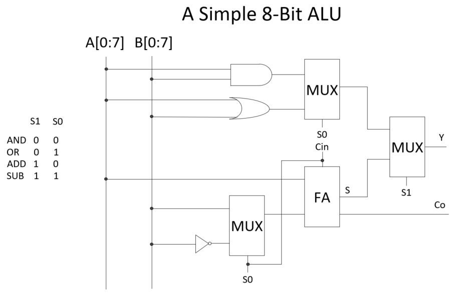
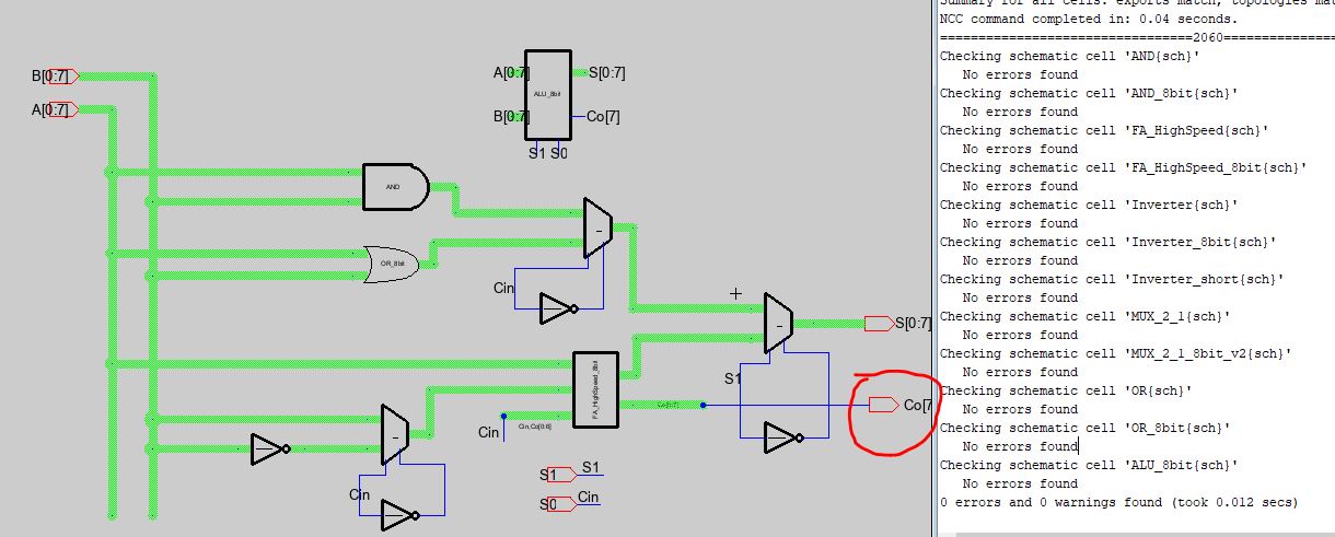
This simple 8-bit ALU can perform AND, OR,
ADDITION (ADD), and SUBTRACTION (SUB) operations. Subtraction is
carried out by inverting the addend and plus 1 (according to 2's
complement).
All the traces in the following figure are buses which carry 8 bits per
trace. The selection bits S1S0 controls the data to be delivered to Y.
When S1S0 = 11, the inverted B passes the MUX as the addend for the FA.
In the meantime, S0, which is 1, is asserting Cin to add an extra 1 to
the FA. This forms the 'inverting and plus 1' rul for the 2's
complement to convert a positive number into it's negative format,
which implements the subtraction operation.
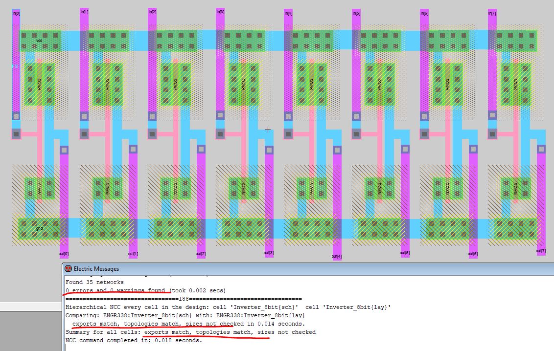
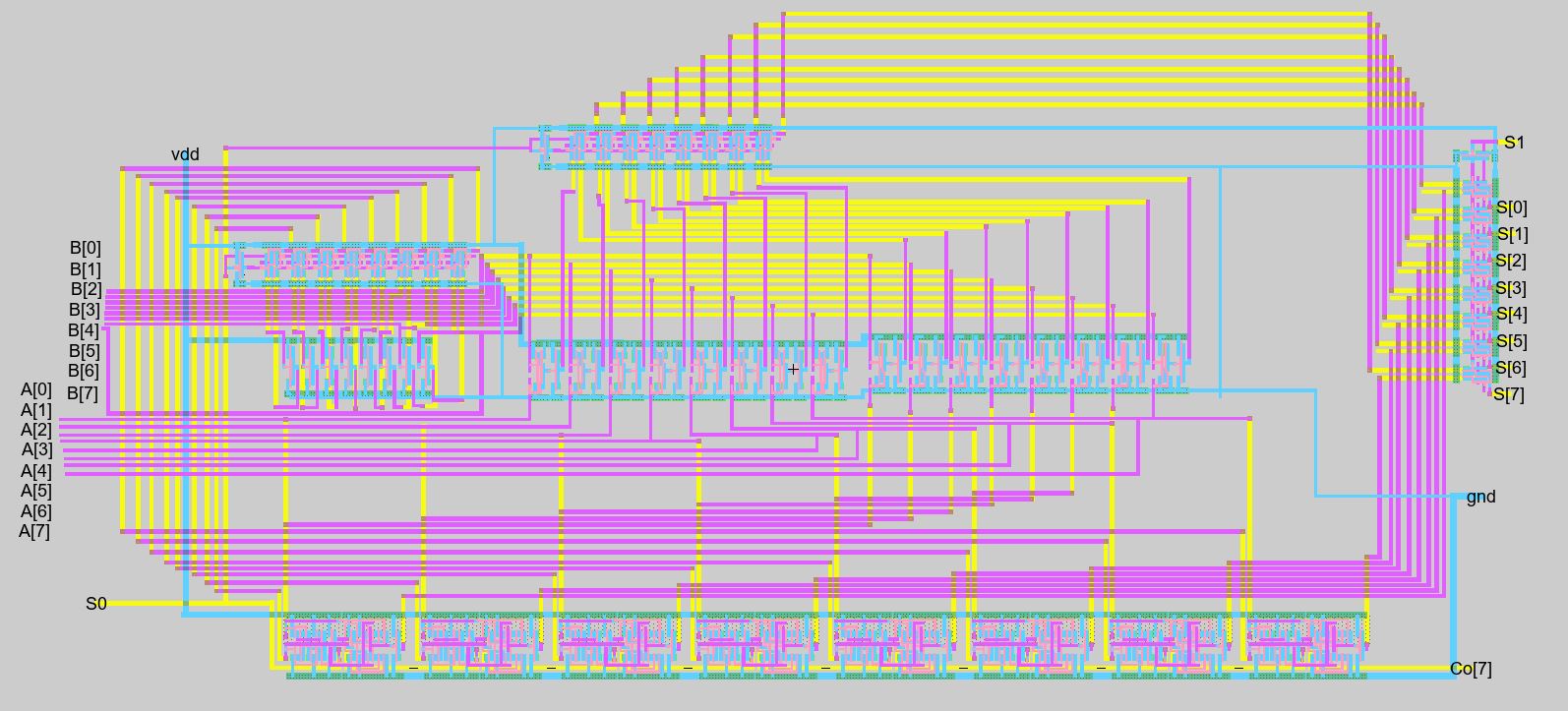
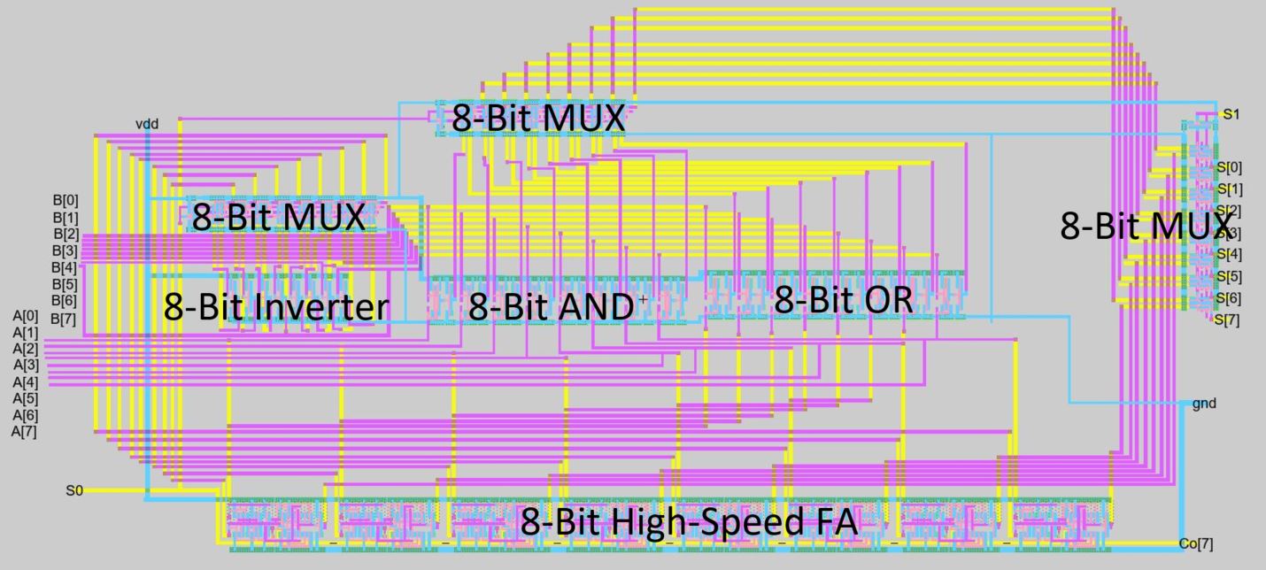
Next, build the schematic in Electric. (You need the 8-bit version of
each module shown in the diagram above). For example I am missing the
8-bit inverter in my library.
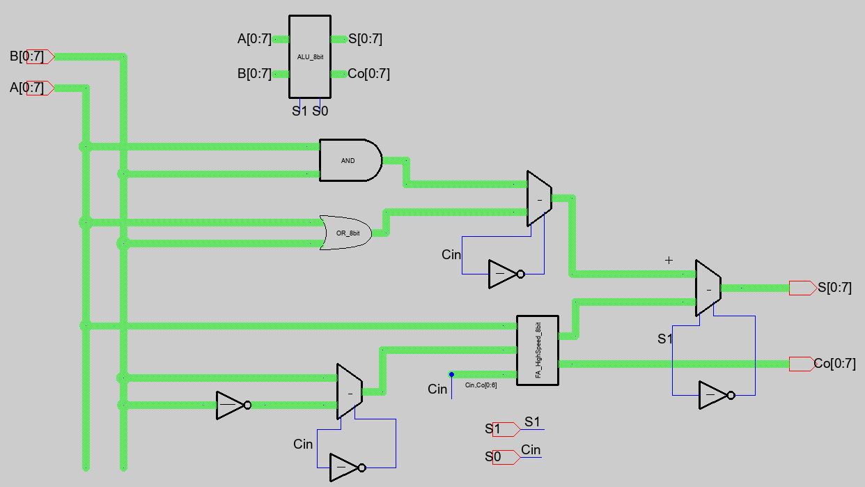
The schematic of the 8-bit ALU:
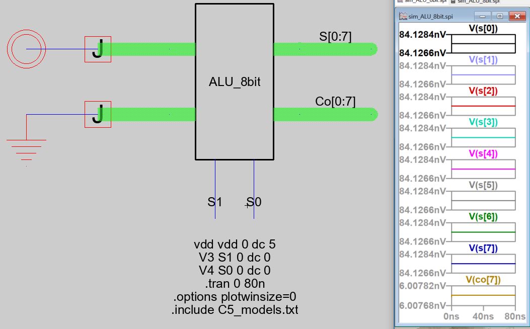
Next, run the simulation:
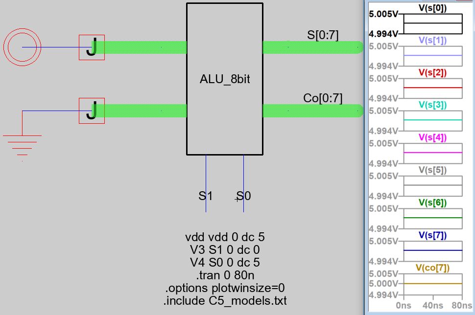
First, verify the AND gate by setting S1S0 = 00:
1111 1111 AND 0000 0000 should be all 0's.
Second, verify the OR gate by setting S1S0 = 01:
1111 1111 OR 0000 0000 should be all 1's.
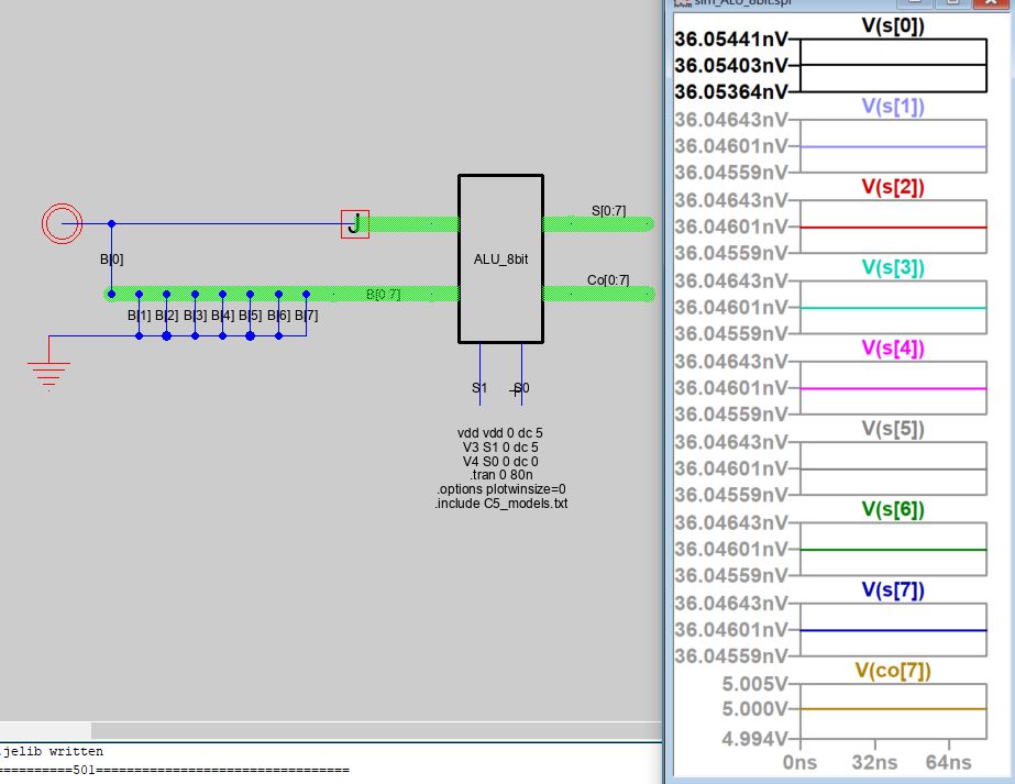
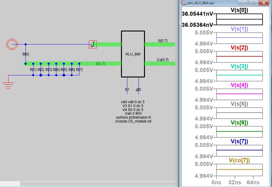
Next, verify the ADD operation. Use 1111 1111 + 0000 0001 = S = 0000
0000, Co = 1.
Watch this short video for the tricks of wiring a large scale
integrated circuit by hand. The rule of thumb is for wiring in between
two modules, keep the traces from the same metal layer consistently
horizontal or vertical.
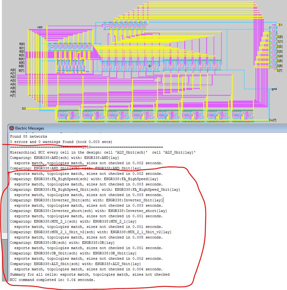
The finished layout looks like this:
I don't need to report all the Co[0:7] ports so I went back to the
schematic to only export Co[7]. Don't forget to make the same changes
to any subcells that are being affected by this change. (like the
simulation one view).
An bigger image of the layout can be seen below (click the figure to
zoom in). One thing to let you know is at some point, you should start
designing this on your own instead of following what I have in the
example. Your layout and location of the ports canbe totally different.
If you just follow mine, you may run into errors and troubles.
Start think about the topology and the design by yourself starting from the schematic in Task 1.