Lab 7 Using Buses in ElectricVLSI
Objectives:
1. Be able to build a ring oscillator use buses.
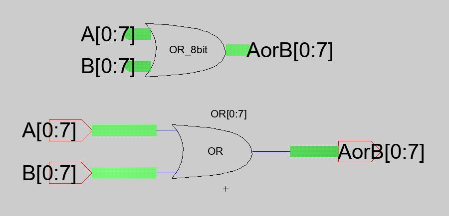
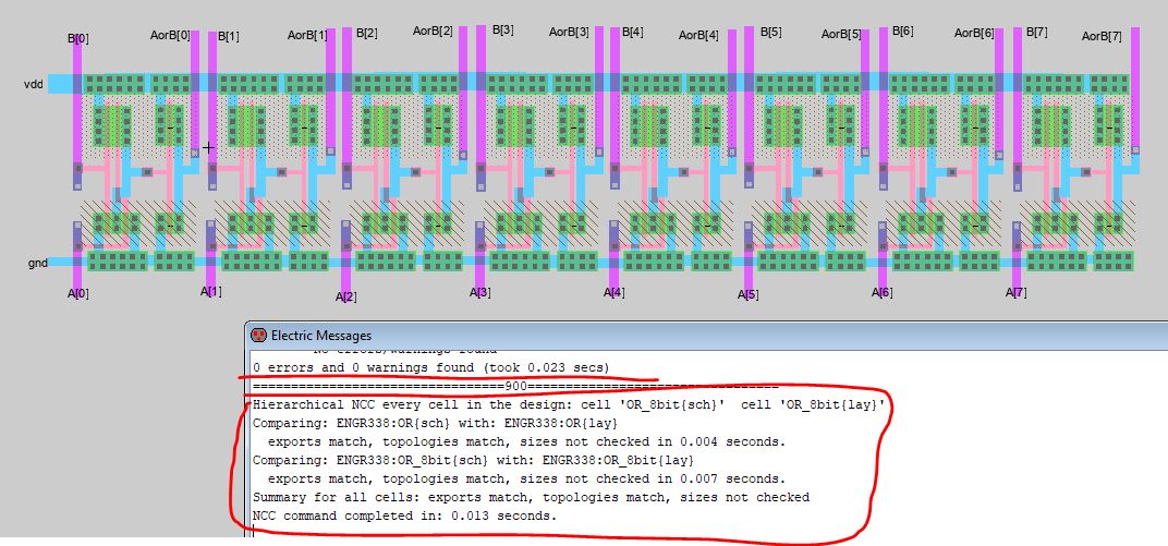
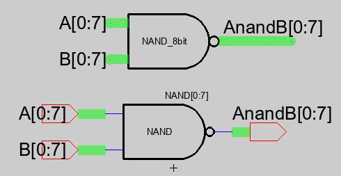
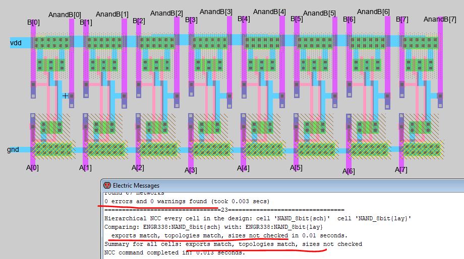
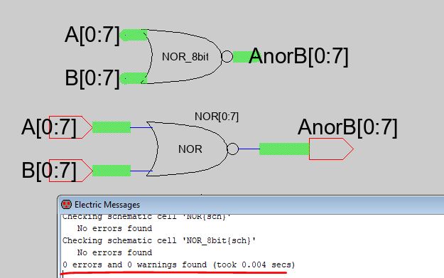
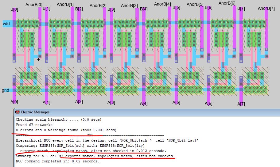
2. Be able to build multi-bit gates in ElectricVLSI.
Lab Tasks:
Task 1: Build and simulate a Ring oscillator. (20 points)
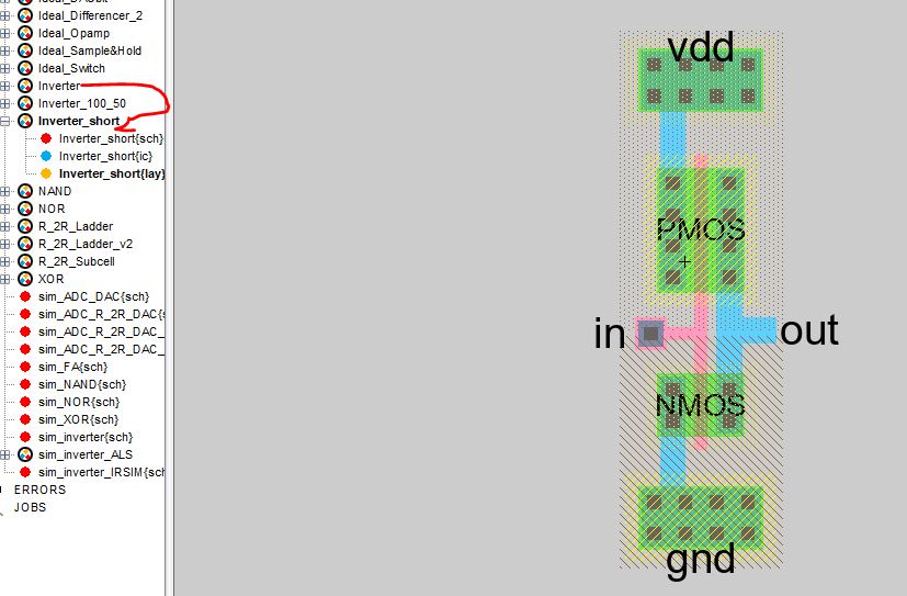
Duplicate the tall inverter cell you created in Lab 4, rename it as 'Inverter_short'. Move the vdd/gnd rails closer to the MOSFETs. Then run DRC/NCC before moving forward.
Create a new schematic view 'Ring_Oscillator'. Drag 'Inverter_short' icon to the view.

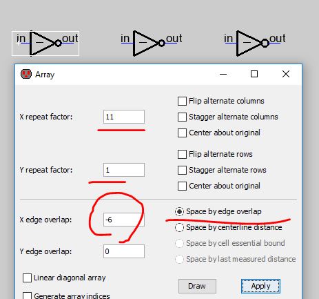
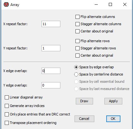
Select the icon by left clicking it and press 'F6' to open the Array setup window. The number '-6' means the inverters are being set apart. This setup creates 11 inverters in a row.
Connect them as a ring. I named the net at the very right hand side as 'osc_out' for LTSpice probing. You can pick up any node inside the ring for display.
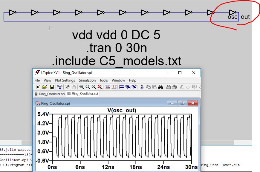
Next, let's build this in a different way (use data buses). Again, create a new schematic view 'Ring_Oscillator_Bus'.
Select the inverter, press Ctrl + i to name it as 'inverter[0:10]'. This will create 11 inverters in parallel virtually. It still shows a single one in the view but there are 11 ones being created in the netlist. [0], [1], [2], ...... [10].
Use the bus to connect the inverter to an input pin and an output pin. Export the input pin as 'osc_out,out[0:9]' and the output pin as 'out[0:9],osc_out'.
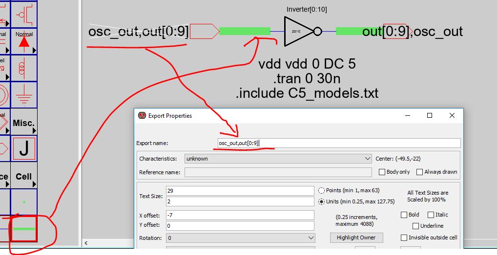
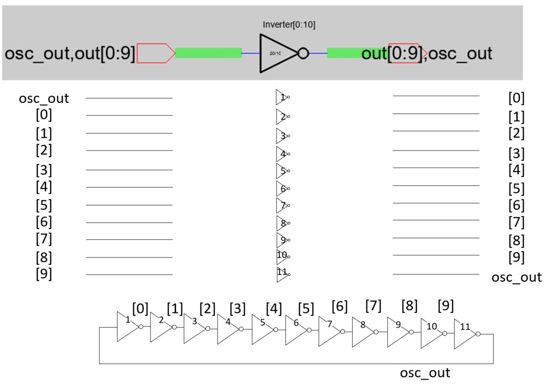
The input pin and the outpin are named as above is because in a ring oscillator, the output of a inverter is shorted to the input of the next inverter. The following diagram shows the input/output connections of each inverter in this array.
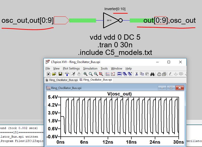
If the schematic is DRC clean, use the same Spice code to run the simulation. It shows the same results as the previous one.
Next, the layout. Use buses is not an option in the layout view. Please explain why in your report.
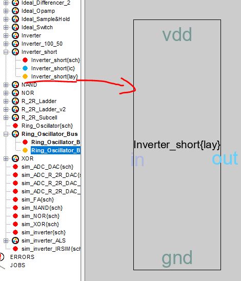
Drag the 'Inverter_Short' to the new layout view.
Make an array out of it.
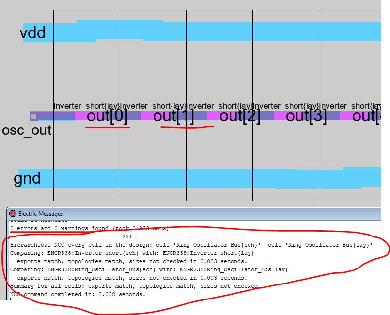
Connect them in as a ring. Use Metal 1 to Metal 2 via at the left and the right side of the row and then use Metal 2 to close the loop. DRC it before you export the pins for LVS.

You must export all the 'out[0] - out[9]' ports to pass the LVS.
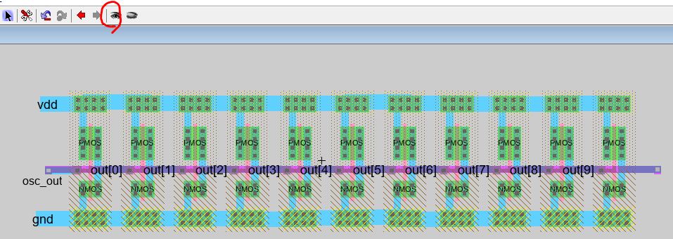
Show the internal circuit of the inverter:
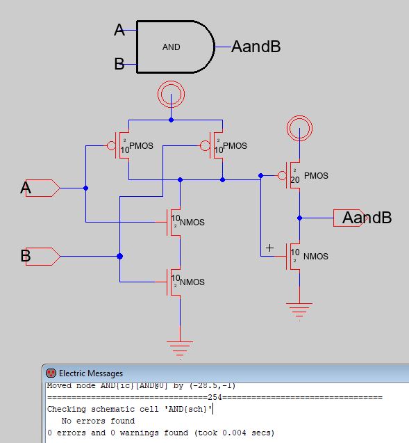
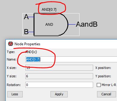
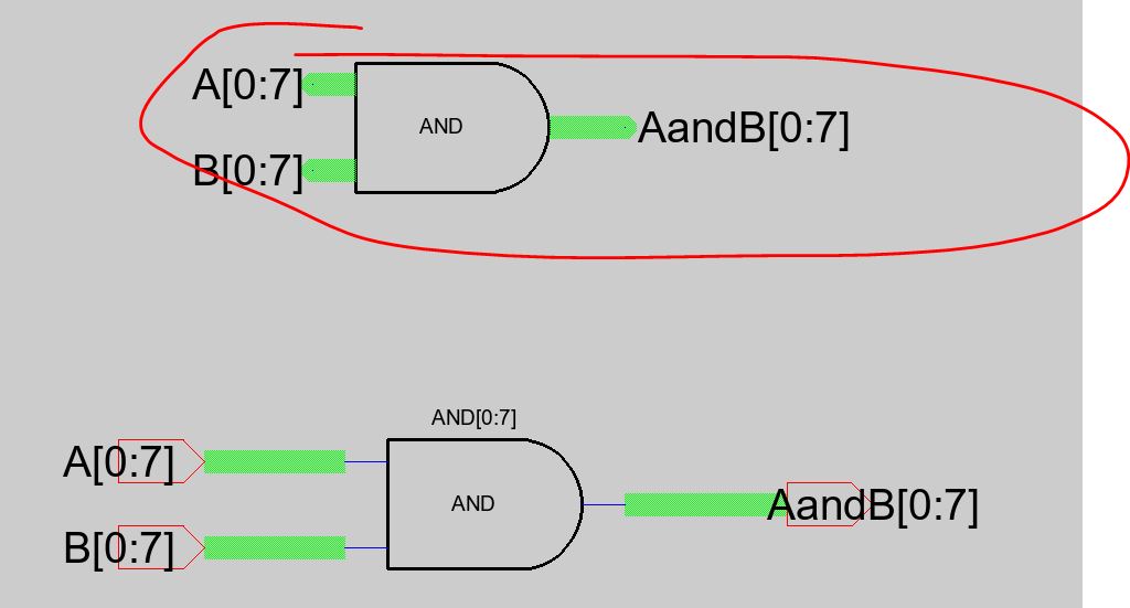
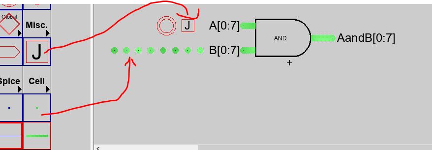
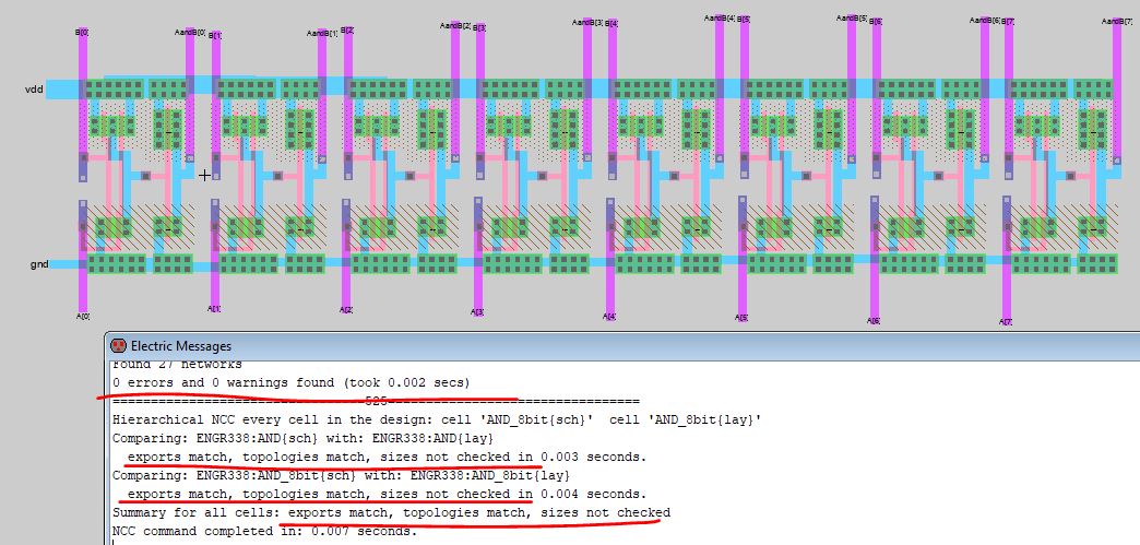
Task 2: Design an 8-bit AND gate.
