ENGR337 Lab 2020 Spring
Lab 9:Tutorial 4
Name: Ryan Ford
Email: rwford@fortlewis.edu
Introduction:
The purpose of this lab was to familiarize students with ElectricVLSI
by having them run through a series of excercise to create a printable circuit board.
Materials and Methods:
The materials used in this lab included LTspice and ElectricVLSI.
Follow the instructions specified in Lab 9, tutorial 4 on yilectronics.com.
Results:
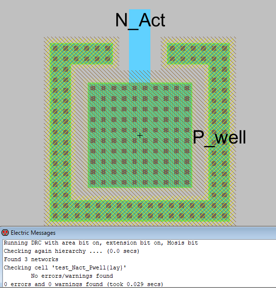
Figure 1 shows the layout view of the Nact Pwell, and Figure 2 shows the schematic view of the Nact Pwell..
Figure 1: Layout view of Pact Nwell
Figure 2: Schematic of Nact Pwell
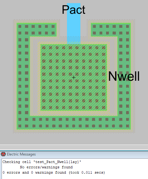
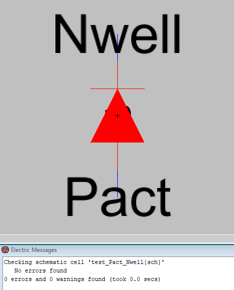
Figure 3 shows the layout view of the Pact Nwell, and Figure 4 shows the schematic view of the Pact Nwell.
Figure 3: Layout view of Pact Nwell
Figure 4: Schematic of Pact Nwell
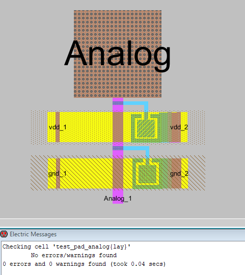
Figure 5 shows the layout view for the analog pad, and Figure 6 shows the schematc view.
Figure 5: Layout view of analog pad
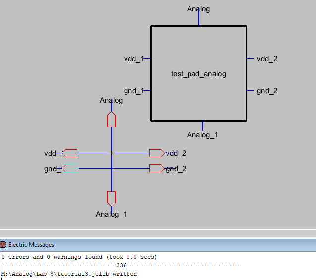 Figure 6: Schematic of analog pad
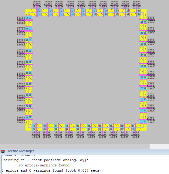
Figure 7 shows the layout view of the anlog padframe, and Figure 8 shows the schematic.
Figure 7: Layout view of analog padframe
Figure 8: Schematic view of analog padframe
Discussion:
All
of the results matched the expected resuts
shown in Lab 9, tutorial 4 on ylectronics.com. It can be seen in
the figures that every schematic and layout are free of errors and
warnings.