ENGR337 Lab 2020 Spring
Lab 5 Recitifiers and DC Regulators
Name: Ryan Ford
Email: rwford@fortlewis.edu
Introduction
This lab
chalenged students to build and simulate circuits to gain a better
understanding of diodes. Diodes were used in all circuits, and
the input and output signals were probed and simulated in LTSpice. The
students were also challenged to explain the results.
Materials and Methods
Table 1: List of Materials
Build the circuits shown in
Lab 5 on yilectronics.com. Probe the input and output signals using an
oscilloscope, and simulate the circuits using LTspice. Compare and contrast the results.
Results
Task 1
1.1)
Figure 1: Circuit 1.1 showing built-in potential of the diode
1.2
Figure 2: Circuit 1.2, showing difference in input and output aafter changing built-in potential
1.3)
 Figure 3: Circuit 1.3, showing input amplitude for built-in potential comparison
 Figure 4: Circuit 1.3, showing output ampitude for built-in potential comparison
Task 2
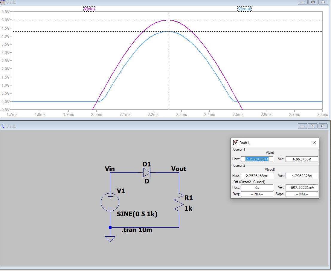
2.1)
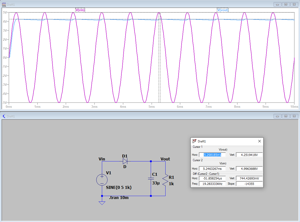 Figure 5: Circuit 2.1, showing difference in input and output voltage
2.2)
Figure 6: Circuit 2.2, showing input amplitude for difference in input and output voltage
Figure 7: Circuit 2.2, showing output amplitude for difference in input and output voltage
Task 3
3.1)
Figure 8: Circuit 3.1, showing differenc in input and output voltage.
3.1a)
 Figure 9: Circuit 3.1 built on breadboard and analyzed with oscilloscope, showing input voltage
3.1b)
 Figure 10: Circuit 3.1 built on breadboard and analyzed with oscilloscope, showing input voltage
3.2)
Figure 8: Circuit 3.2, showing difference in inout and output voltage
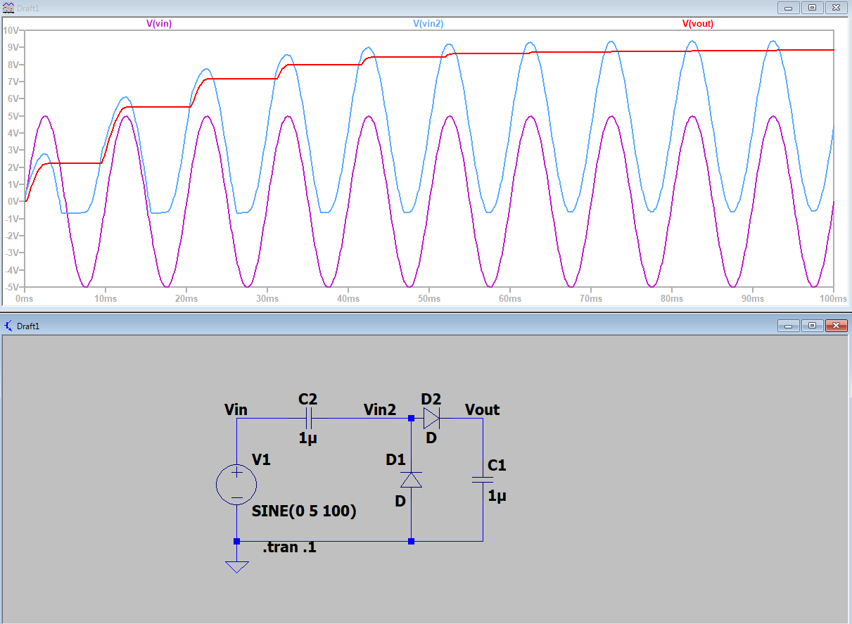
Task 4
Figure 9: Circuit 4, showing difference in input and output voltages of voltage doubler circuit
Figure 10: Circuit 4 built on a breadboard, showing input and output voltages
Discussion
Task 1: The built-in voltage for circuit 1.1 is .7V. After
adjusting the built-in voltage to be .6V, the results were as
expected. The circuit was built on a breadboard, using a 1N 5767
diode, and the built-in potential of the diode was determined to
be about .74V.
Task 2: Circuit 2.1 was modeled in LTspice and the
difference in input voltage and output voltage was found to be about
.75V. The output voltage displayed a large difference in wave
behavior, indicating the capicator was not
diasharging. The circuit was built on a breadboard, and the
oscilloscope readings looked similar to the LTSpice simulations.
Task 3: Circuit 3.1 was simulated in LTSpice,
and the results showed a reduction in voltage from the resistor.
The results also show what we would expect from having two diodes in
oposite directions. As the sin wave increased, the voltage
increased until reaching the Built-in voltage, then it was
constant. The same occured as the sine wave decreased for the
reverse biased diode. The results in the breadboard circuit
very closely simulated the LTSpice results.
Task 4: Circuit 4 represents a classic voltage doubler
circuit. Th results show an output voltage that is twice the
input voltage, however the output voltage is DC.