ENGR337 Lab 2020 Spring
Lab 2: More LTSpice and the Compensated Probe
Name: Ryan Ford
Email: rwford@fortlewis.edu
Introduction:
The pupose of this lab was to further familiarize students with circuit
analyses in LTSpice, as well as by hand and with tools such as an
oscilloscope. Additionally, the lab helped increase the students'
understanding of the mechanisms of compensated oscilloscope probes.
Materials and Methods:
Table 1: Materials list
Build the circuits as shown in the Lab 2 section on yilectronics.com. Analyze
the circuits by running simulations in LTSpice, following instructions
according to Lab 2. Perform hand calculations as required, and compare
results with measured and simulated data.
Results:
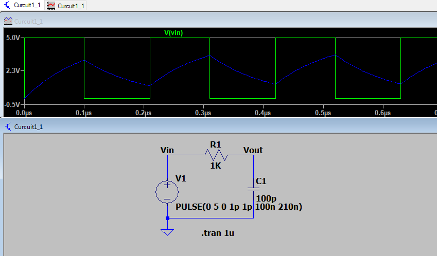
1.1)
Figure 1: 1.1 circuit with LTSpice analyses
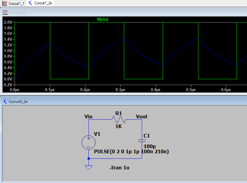
1.2a)
Figure 2: 1.2a circuit with LTSpice analyses
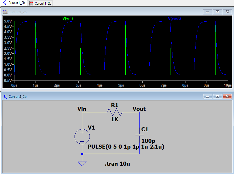
1.2b)
Figure 3: 1.2b circuit with LTSpice analyses
Figure 4: 1.2c circuit with LTSpice analyses
1.2d)
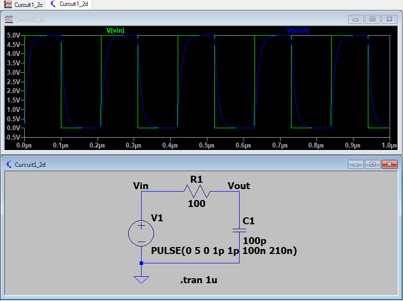 Figure 5: 1.2d circuit with LTSpice analyses
1.3)
Figure 6: 1.3 circuit with oscilloscope analyses
2.1)
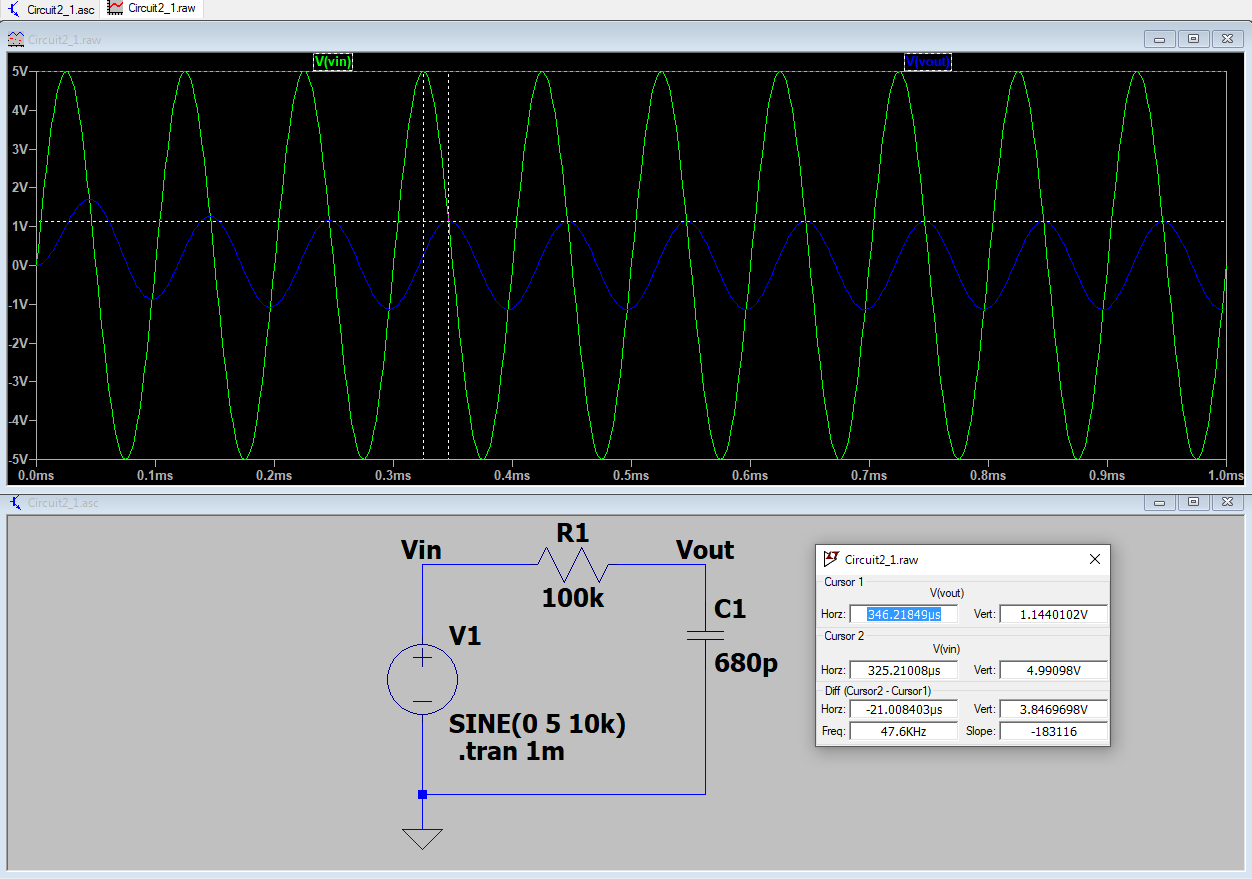
Figure 7: 2.1 circuit with LTSpice analyses

Figure 8: 2.1 circuit with oscilloscope analyses
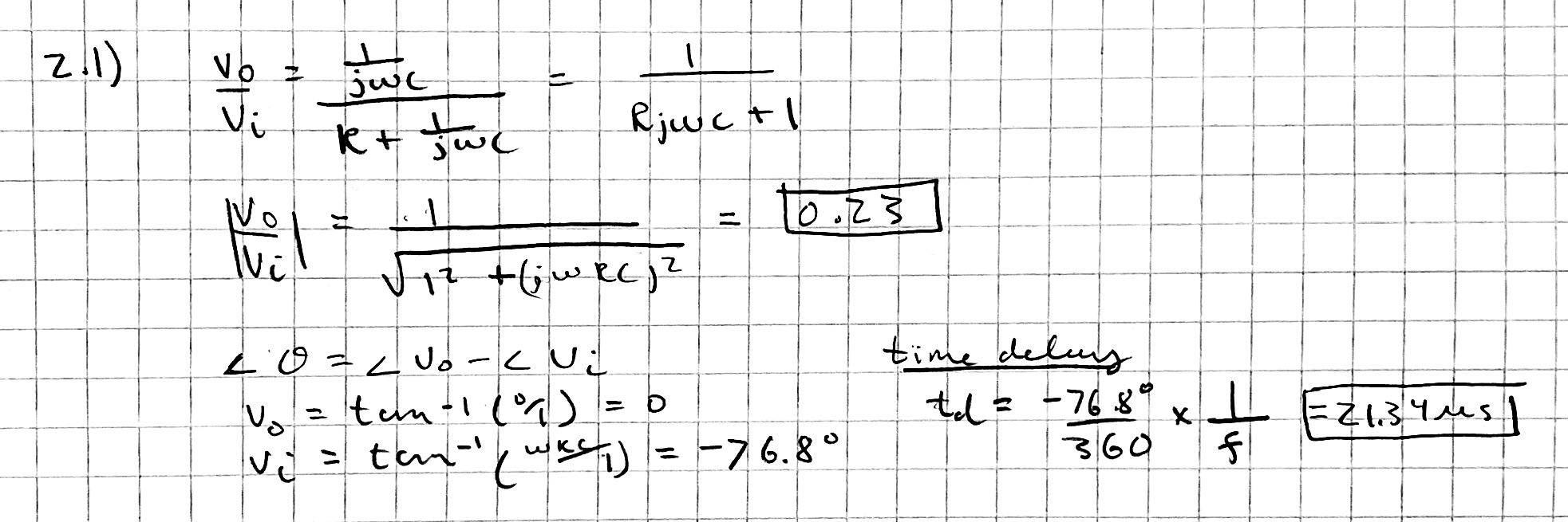 Figure 9: 2.1 circuit hand-calculations
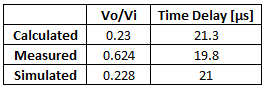
Table 2: Calculated vs measured vs simulated results for 2.1
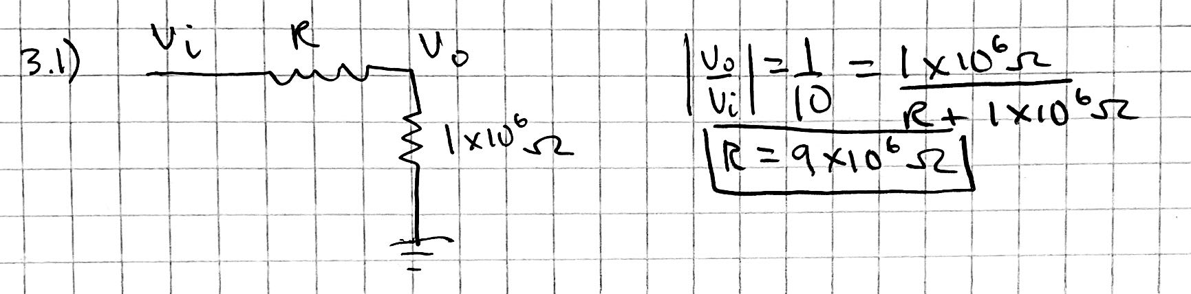
3.1)
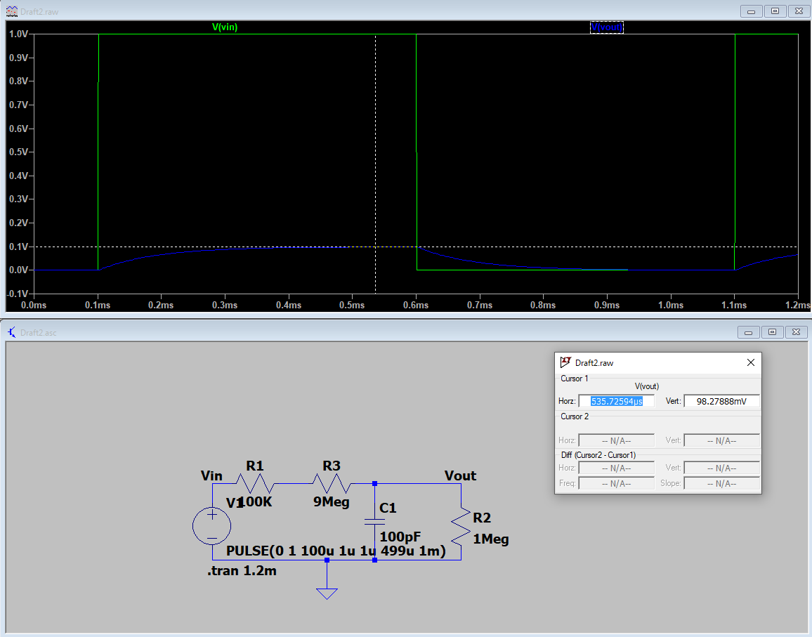
Figure 9: 3.1 circuit with oscilloscope analyses
Figure 10: 3.1 circuit hand calculation
3.2)
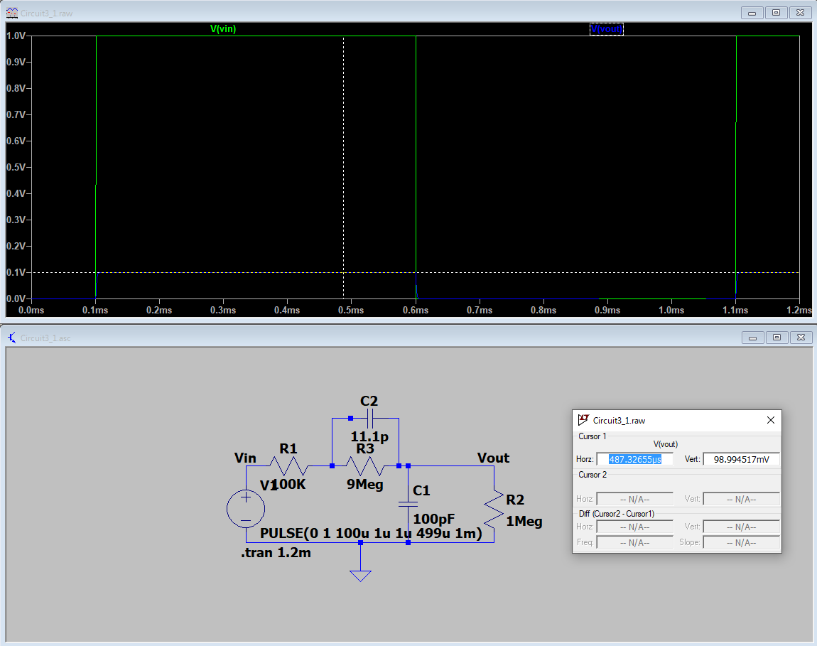
Figure 11: 3.2 circuit LTSpice analyses
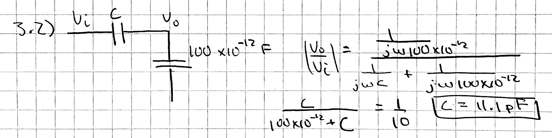 Figure 12: 3.2 circuit hand calculation
3.3)
The oscilloscope probes were of the type 10:1. If changed to 1:1, the detected voltage values would be 10x smaller.
5. Discussion
The circuit in 1.1 displayed results indicating that the capacitor was
not able to charge or discharge fast enough to reach maximum voltage
potential. In 1.2a, changing the voltage input did not change the
results from 1.1. in 1.2b, the pulse period was changed and that
allowed the capacitor to charge and discharge completely.
Circuit 1.2c shows that decreasing the capacitance is a possible
to solution to let the circuit charge and discharge completely.
Circuit 1.2d shows that changing the resistance can also effect the
voltage output. Circuit 1.3 gave us expected results. In
2.1, the time delays were all very similar, but the attenutation was
different when measured using the oscilloscope; this is indicative of
the internal resistivity of the probes. Circuits 3.1 and 3.2 were
designed by hand calculations and verified in LTSpice.