ENGR337 Lab 2020 Spring
Final Project
Name: Ryan Ford
Email: rwford@fortlewis.edu
Introduction:
The purpose of this project was to familiarize students with
ElectricVLSI
and circuit design by having them run through a series of excercise to
create a printable circuit board. The final circuit board is an
inverting op amp. The project challenged students to learn debugging
techniques, as well as develop a better understanding of transistors
and op amps.
Materials and Methods:
The materials used in this lab included LTspice and ElectricVLSI.
After completing tutorials 1 through 4, follow the instructions specified in tutorial 5 on yilectronics.com.
Results:
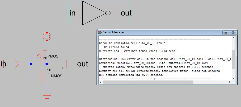
Figure 1 shows the schematic of the inverter, and Figure 1a shows the
layout of the inverter. As seen in both figures, DRC and NCC are
clean.
Figure 1: Inverter schematic view
Figure 1a: Inverter layout view
Figure 2 shows the schematic of the bias circuit, and Figure 2a
shows the layout view of the bias circuit. As seen in both
figures, DRC and NCC are clean.
Figure 2: Bias circuit schematic
Figure 2a: Bias circuit layout
Figure 3 shows the schematic of the op amp circuit, and Figure 3a shows the layout view. As seen in the figures, DRC and NCC are clean.
Figure 3: Op amp schematic
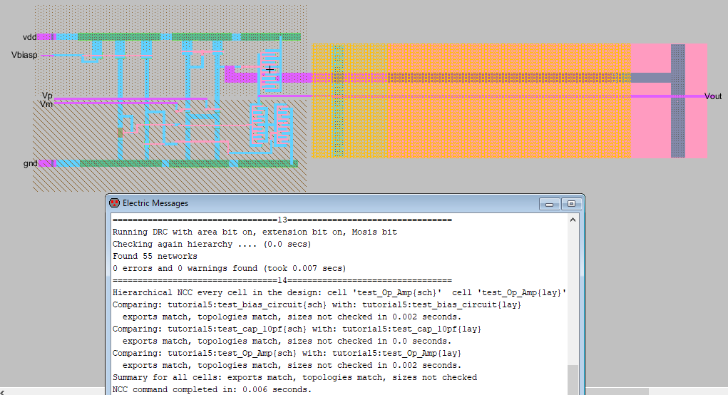 Figure 3a: Op amp layout
Figure 4 shows the schematic of the final ESD chip, and Figure 4a shows
the layout. It can be seen in the figures that final project was
completed without DRC or NCC errors.
Figure 4: Final ESD chip schematic
Figure 4a: Final ESD chip layout
Discussion:
All
of the results matched the expected resuts
shown in tutorial 5 on ylectronics.com. It can be seen in
the figures that every schematic and layout are free of DRC and NCC
erros. This project was a challenge of patience and attention to
detail. Skills in troubleshooting ElectricVLSI were developed
during the process of creating this chip.