1. A Padframe with ESD Protection 2. In this lab, students continued to learn how to build and assemble electrical components in ElectricVLSI.
An N-Act. P-Well diode was constructed first followed by a P-Act,
N-Well diode. These components were used to create an analog pad with
built-in ESD protection which was finally used to construct a padframe
for use in the final project for the class. This lab covered the
information present in Tutorial 4. Only 2 more
ElectricVLSI tutorials remain before students begin the final project
for this class.
3. Materials
LTSpice
software (for simulation)
ElectricVLSI Software
Java (for running ElectricVLSI)
Methods Students
began the lab by opening the tutorial_3.jleb file to and creating a new
layout cell for the N-Act, P-Well diode. This library was resaved as tutorial_4.jleb. The C5 process was
once again used for this lab. Students
followed along with an instructional video Dr. Li created to guide them
through the creation of an N-Act, P-Well diode and a P-Act, N-Well
diode. Students created a layout and schematic cell for both diodes.
The N and P Wells as well as the N and P Active areas were properly
sized and arranged and their pins were exported. Students continued on
to the second video where they were directed to create a single pad
with electrostatic discharge (ESD) protection. The diodes created
during the previous video were incorperated into the pad and wired to
metal layers 1, 2, and 3 in the proper configuration. This process was
more involved than the diode creation phase of the lab. The components
were created to the specifications laid out in the second video posted
byDr. Li. The pins for vdd, gnd, and Analog connections were exported.
The DRC and NRC verifcations were run in ElectricVLSI to ensure the
schematic and layout cells corresponed and no errors were present. An
icon cell of the pad was also created. The lab concluded with the
creation of the analog padframe that sutdents will use to design their
analog chips for the final project of the class. Students followed
along with a third video posted by Dr. Li as they designed their
padframes. The padframe incorperated the pad previously designed. The
pad was put into an array of 10 pads algined horizontally and copied
three times to form the square of the padframe. The pads had to be
properly aligned and their metal 3 connections properly wired to ensure
the frame stayed within the specified dimensions of the video. A DRC
check was run to ensure no notch errors were present. The vdd and gnd
connections of each pad were wired together to complete the padframe
layout. A schematic of the pad frame was then created using the same
array process and alginment as seen in the layout. The pad icon was
used to create this schematic. The vdd and gnd pins of each pad were
wired together in the schematic just like they had been in the layout.
The jleb file was saved and the tutorial concluded.
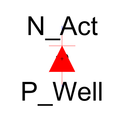
4. Results Figure 1. The
completed schematic for the N-Act, P-Well diode as specified in the first video (provided by Dr. Li).
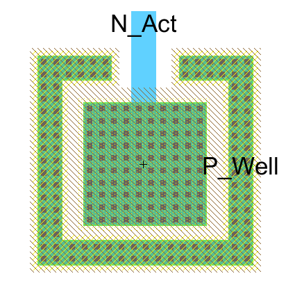
Figure 2. The
completed layout for the N-Act, P-Well diode as specified in the first video (provided by Dr. Li)..
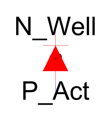
Figure 3. The
completed schematic for the P-Act, N-Well diode as specified in the first video (provided by Dr. Li)..
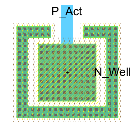
Figure 4. The
completed layout for the P-Act, N-Well diode as specified in the first video (provided by Dr. Li).
Figure 5. The
completed schematic for the ESD protected pad as specified in the second video (provided by Dr. Li).
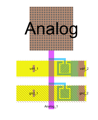
Figure 6. The
completed layout for the ESD protected pad as specified in the second video (provided by Dr. Li).
Figure 7. The
completed icon for the ESD protected pad as specified in the second video (provided by Dr. Li).
Figure 8. The
completed layout for the ESD protected padframe as specified in the third video (provided by Dr. Li).
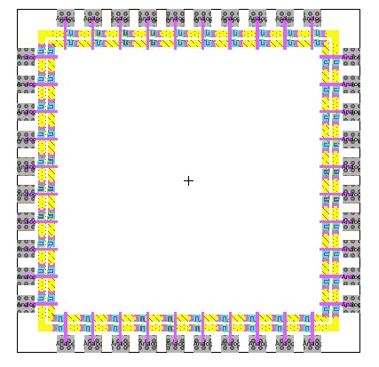
Figure 8. The
completed layout for the ESD protected padframe as specified in the third video (provided by Dr. Li). This layout will be used in the final project for this class.
5. Discussion This
lab was the fourth of six labs designed to teach students the
skills they need in ElectricVLSI to complete the final project for this
class. Tutorial Four introduced students to the creation of the ESD
protected padframe they will be using for their final projects. The
uses of N-Act, P-Well diodes and P-Act, N-Well diodes were also
introduced to students. The important role they play in protecting the
circuit present on the padframe was explained by Dr. Li and helped
students understand why they were completing certain tasks during the
lab. The first two instructional videos were not hard to follow. The
creation of the diodes and their respective layouts and schematics were
easy for students to complete and very few errors were found by the
VLSI software in these cells. The creation of the pad proved slightly
more difficult and students did have to correct a few errors that
popped up in DRC and NCC verification. The pads had to be altered
several times as well to fulfill the neeeded specifications for the ESD
protected padframe. The padframe proved difficult for students to
complete. The video provided by Dr. Li had to be rewatched in serveral
places numerous times. Multiple errors were found during DRC
verification and the origianl pad layout had to be altered to fix these
errors. Wiring the vdd and gnd proved particularly tedious as the wire
connections would not align correctly and generated notch errors. The
problem took most students over an hour to solve and some students even
had to restart their padframe layouts entirely. The errors and
connection issues were finally solved and the schematic fo the padframe
layout was created. This was much easier for students to complete and
concluded the lab upon completion. Though this lab proved difficult,
student familiarity with the VLSI software proved invaluable as they
were able to call upon previous knowledge from past tutorials to solve
the problems they encountered. The videos posted by Dr. Li were also
extremely helpful to students. This lab marks a major accomplishment in
moving towrds the final project. With the pad frame completed students
are left with desigining their final circuit for the class.