1. Layout of an Inverter 2. In this lab, students continued to learn how to build electrical components in ElectricVLSI.
An inverter layout was created using the NMOS and PMOS MOSFETs
developed in Tutorial 2. The input and output voltages of the inverter
were simulated in LTSpice to verify the inverter was created properly.
This lab covered the information present in Tutorial 3. Only 3 more
ElectricVLSI tutorials remain before students begin the final project
for this class.
3. Materials
LTSpice
software (for simulation)
ElectricVLSI Software
Java (for running ElectricVLSI)
Methods Students
began the lab by opening the tutorial_2.jleb file to copy and paste
their NMOS and PMOS transistors into a new schematic. The transistors
were converted to generic NMOS and PMOS configurations respectively and
the PMOS MOSFET was adjusted to have a length of 20. The C5 process was
used for this lab. The NMOS and PMOS were then wired together and
attached to a power and ground signal. The schematic was then wired to
off-page nodes representing the input and output voltages. An icon view
for the schematic was then created and altered to match the look of a
conventional inverter symbol. This icon was transported to its own cell
and wired to accept a Spice code input voltage. The output was also
wired to verify the inverter was correctly constructed in ElectricVLSI.
The Spice code was run and a graph of the input and output voltages
were displayed and compared to the graph generated by Dr. Li. A layout
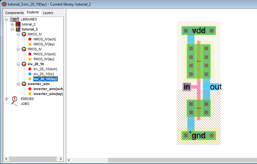
of the inverter was created and the necessary components were assembled
to match the specifications of the 20-10 inverter sechmatic. Once the
layout was completed the pins for the input voltage, output voltage,
ground, and vdd were exported. Another layout was generated to create a
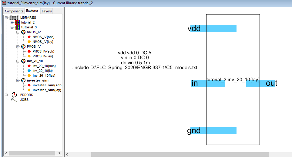
more user-friendly means of circuit simulation. This layout was wired
and the pins were exported to match the pins of the intial inverter
layout. Spice code was included with this layout to simulate it upon
completetion. The inverter layout was simulated and compared to both
the simulations of the inverter icon and Dr. Li.
4. Results Figure 1. The
completed schematic for the inverter using the NMOS and PMOS developed
in Tutorial 2. The icon veiw is present in the top right as well.
Figure 2. The completed icon
for the inverter schematic along with wired input and output
connections and Spice code needed for simulation.
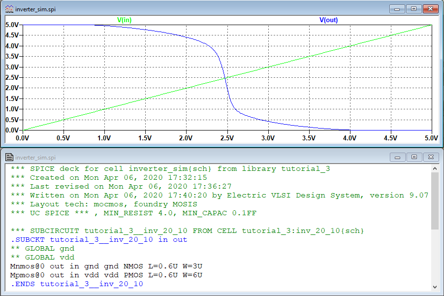
Figure 3. The LTSpice simulation for the inverter schematic with input and output voltages compared.
Figure 4. The completed layout for the inverter along with wired connections and exported pins.
Figure 5. The simplfied
layout of the inverter. This layout was created to help users easily
simulate the more complicated layout developed in the previous figure.
Spice code is also present for intializing simulation.
Figure 6. The LTSpice simulation for the inverter layout with input and output voltages compared.
5. Discussion This
lab was the third of six labs designed to teach students the
skills they need in ElectricVLSI to complete the final project for this
class. Tutorial Three introduced students to the creation of inverters
as well as built on their knowledge of NMOS and PMOS MOSFETs. The
concept of creating icons to represent more complicated ciruit
components was also introduced. Students demonstrated the growth of
their skills in the VLSI software as they created
circuit layouts and schematics with less instruction than the previous
two labs. Student familiarity with the software resulted in the lab
being completed in less time than the previous labs. The inverter was
constructed correctly and simulated two times to ensure it behaved as
expected. The circuit successfully inverted the input voltage in both
simulations. The use of DC to AC inverters allows many devices used by
people everyday to function properly. It is with programs like
ElectricVLSI this circuits are designed and preapred for production and
use in many pieces of techology. Students continued to learn the
importance of analog circuitry in this lab as well as develop their own
personal design skills and understanding of these circuits. The
information learned during this lab will prove valuable to students in
completing future labs, their final projects, and possibly their future
careers.