1. MOSFETs and IV Curves 2. In this lab, students continued to learn how to build electrical components in ElectricVLSI.
A single NMOS and PMOS MOSFET were created for the C5 process. The IV
curve of each device was examined and compared. This lab contains the
work completed from Tutorial 2 of the 6 tutorials students must
complete before beginning the final project for this class.
3. Materials
LTSpice
software (for simulation)
ElectricVLSI Software
Java (for running ElectricVLSI)
Methods Students
began the C5_models.txt file found on Dr. Li's Website. This file
contained the models required to simulated the completed NMOS and PMOS
circuits. The file was saved to the same directory as ElectricVLSI and
a new schematic was created for creating the NMOS circuit. AN NMOS
circuit was inserted into the schematic and a spice model was assigned
to it. The NMOS node was assigned to the NMOS spice model. Another
layout was created and a PMOS node was inserted into it. The PMOS spice
model was assigned to the node. Next, both the NMOS and PMOS nodes were
edited in ElectricVLSI to their respective 4 port devices so simulation
could be carried out. Both schematics were saved and a layout for
the NMOS device was created. An NMOS and two N-nodes were placed in the
layout and connected. A metal contact was added to the layout followed
by a P-well node functioning as the body connection for the device. The
NMOS in the layout was also set to spice model NMOS for simulation.
Both N-wells and the P-well were edited to match the x-dimension for
the NMOS itself. The nodes were connected with arcs and the arcs were editing to the correct size for each connection. The
layout was cecked for errors. If errors were detected in the VLSI, they
were immediately fixed. The pins were exported to their respective
ports (ie gnd, d, s, etc.). The layout was saved and the process was
repeated for the PMOS device with its corresponding wells and pins.
Spice code was entered into each layout once they were completed and a
simulation was conducted. The schematics for both the PMOS and NMOS
were altered to correspond with their respective layouts and saved upon
completion.
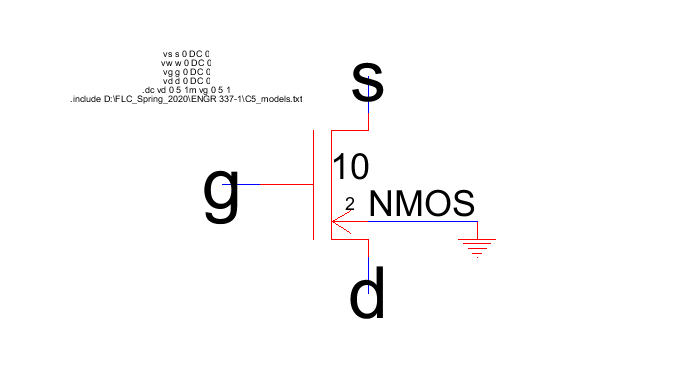
4. Results Figure 1. The completed schematic for the NMOS MOSFET as prescribed in Tutorial 2.
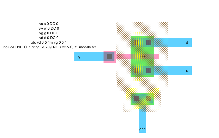
Figure 2. The completed layout for the NMOS MOSFET as prescribed in Tutorial 2.
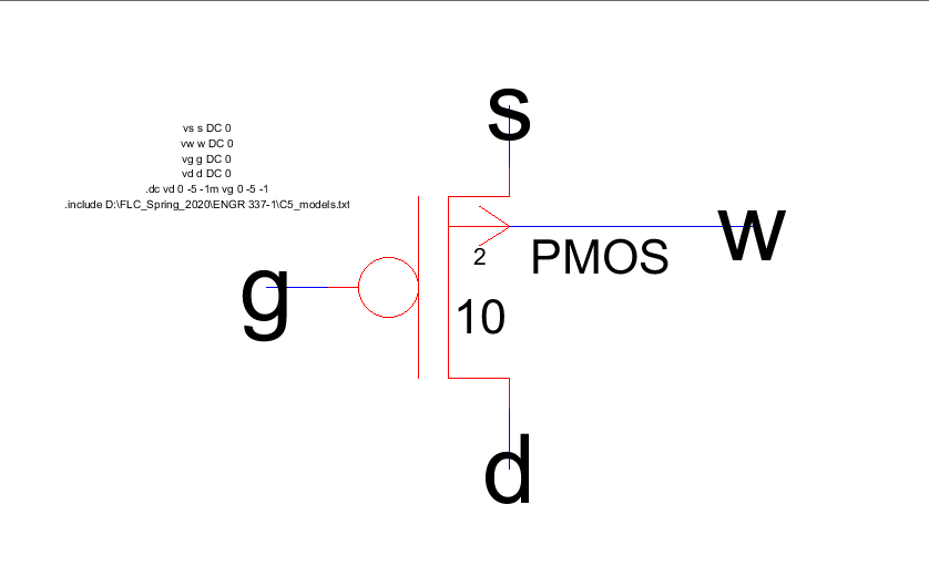
Figure 3. The completed schematic for the PMOS MOSFET as prescribed in Tutorial 2.
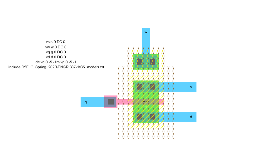
Figure 4. The completed layout for the PMOS MOSFET as prescribed in Turotial 2.
Figure 5. The LTSpice simulation conducted for the completed NMOS MOSFET as prescribed in Tutorial 2.
Figure 6. The LTSpice simulation conducted for the completed PMOS MOSFET as prescribed in Tutorial 2.
5. Discussion This
lab is the second of a series of labs designed to teach students the
skills needed in ElectricVLSI tom completed the final project for this
class. Tutorial Two continued to develop student ability to create
layouts and schematics as well as familiarize students with the overall
software. The NOMS and PMOS MOSFETs took the entire lab periods to
complete but were simple to construct overall. A few errors were
ecnountered by students when tyring to simulate the MOSFETs. Most of
these errors were due to the pins not being exported correctly ir arcs
that were misaligned. The errors were easily corrected with the help of
Dr. Li. The simulations showed that the currents for the NMOS and PMOS
were equal in magnitude but active in different voltage regions. The
NMOS device produced a current while the input voltage was positive.
The PMOS device produced a current while the input voltage was
negative. This shows how each transistor is needed to operate an
electrical device correctly as they each can cover half of an input AC
signal. This tutorial was slightly more complex than Tutorial One and
helped students prepare for the tasks they will need to complete in the
upcoming turorials. The future labs will continue to
build on the base of knowledge gained from Tutorial Two as students
slowly prepare to begin the final project for the class.