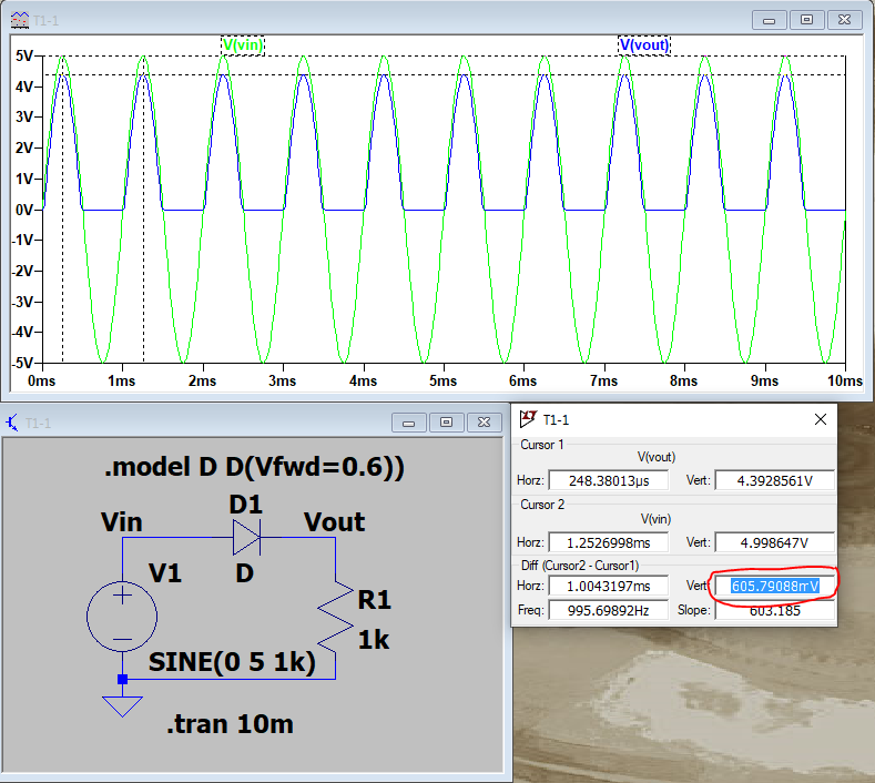
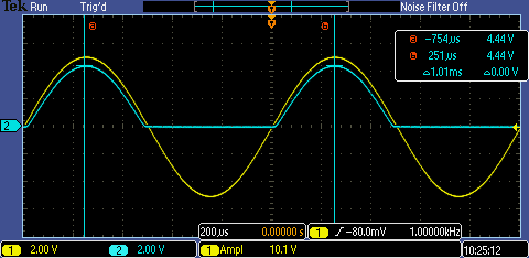
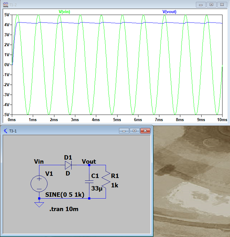
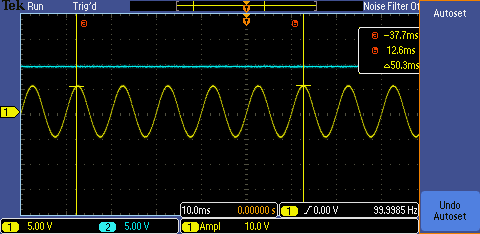
ENGR337 Lab 2020 Spring
Lab 5 xxxxxx
Name:
Orion Clay
Email: oeclay@fortlewis.edu

1. Rectifiers and DC Regulators

2. In this lab,
students learned how to construct rectifier and DC regulator circuits in LTSpice and on a breadboard. Diodes wer introduced to a lab for the first time to accomplish this and students learned how to proeprly incorperate them into a circuit. The concept of a voltage multipier was also introduced and students constructed a multiplier circuit and used it to multiply an input voltage.

3. Materials
Tektronix MSO 2022B Mixed Signal Oscilloscope
Multimeter probe (for circuit debugging)
LTSpice software (for simulation)
Bread Board Two 1N 5767 Diodes
Two 1n5230 Zener Diodes
One 1k Ohm Resistor Two 1 uF Capacitors
One 33 uF Capacitor
Tektronix AGF1062 Arbitrary Function Generator


**All cables necessary for taking measurements with the above devices were used in this lab.**

Methods
Students began the lab by simulating a circuit in LTSpice with a 0-5 volt sine wave input , a 1k resistor, and diode. The built-in voltage of the diode was measured and reported. Students then changed the built-in voltage of the diode by writing a line of spice code and simulated the circuit again.
Students reviewed the data sheets provided by Dr. Li regarding the diodes and zener diodes to find the correct anode and cathode for circuit construction. The circuit was then built on a bread board and the input and output were measured with an oscilliscope. The built-in voltage for this circuit was reported. Students next simulated a rectifier circuit using a diode, 1k resistor, and 33 uF capacitor and the input and output signals were reported. The circuit was then built on a bread board and probed with the oscilliscope. The third task had students create a half-wave rectifer circuit using two diodes and a 1k resistor in both LTSpice and on a bread board. The input and output signal were recording in LTSpice and probed with an oscilliscope on the bread board. Students then created a circuit using two zener diodes in series facing each other in place of the two diodes from Task 3.1. The breakdown voltage of the zener diodes was set to 10 volts by typing a line of spice code. The input and output were simulated as well as measured by an ocsilliscope after students constructed the circuit on a bread board. To wrap up the lab, students constructed a DC voltage multiplier to multiply a signal provided by a function generator. The circuit was simulated in LTSpice as well as constructed on a bread board and the input and output from both methods were reported.

4. Results

Figure 1. The circuit schematic for Task 1.1 as well as the standard built-in voltage used by LTSpice for diode simulation (0.7 V).


Figure 2.
The circuit schematic for Task 1.2 as well as the spice code for the 0.6 V built-in voltage used in the diode.


Figure 3. The oscilliscope reading for the Task 1.1 circuit constructed on a bread board. The circuit is a half wave rectifier and only outputs the half of the input signal that is positive (Vi > 0). When V1 is above zero, the diode is "on" and the current can flow through it. The slight difference in the peaks is due to the diode built-in voltage (about 0.7 V).


Figure 4. The circuit schematic for Task 2 as well as the measured input and output voltages.


Figure 5. The oscilliscope reading for the Task 2 circuit built on the bread board.


Figure 6. The circuit schematic for Task 3.1 as well as the measured input and output voltages.


Figure 7. The oscilliscope reading for the Task 3.1 circuit built on the bread board. This circuit regulates the AC signal voltage being provided to a voltage around +1V/-1V. It does not impeded the signal because it each diode is "on" for either the positive or negative half of the wave.


Figure 8. The circuit schematic for Task 3.2 as well as the measured input and output voltages.


Figure 9. The oscilliscope reading for the clamped voltage zener circuit. NOTE: The function generator could not supply a 40 volt input signal like specified in the lab so a 10 volt input signal was used instead. The output can be seen being "clamped" at 5 volts by the zener diodes. This ensures the output voltage does not surpass the correct voltage for whatever device is connected to this regulator circuit.


Figure 10. The zener voltage range for the 1N5230 diorde used in Task 3.2.


Figure 11. The circuit schematic of voltage multiplier fo Task 4 as well as the measured input and output voltages.


Figure 12. The oscilliscope reading for the voltage multiplier circuit. NOTE: The  output voltage is a steady line because the oscilliscope takes an intantaneous reading. This shows the multiplied voltage and not the intial ramp up to the multiplied voltage as shown in LTspice.

5. Discussion
The practical applications of analog circuits were once again demonstrated to students upon finishing this lab. Recitfier circuits as well as DC regulators and multipliers help engineers design devices, such as a laptop power-pack, in ways that are effcient and dafe for their intended use. For example, without a DC signal multiplier, a laptop power-pack would require a significant amount of voltage and current from an electrical wall outlet. This would be unsafe for both people and the laptop itself. Because of the circuits that students learned to construct in this lab, modern devices are able to function correctly.