ENGR337 Lab 2020 Spring
Lab 2 xxxxxx
Name:
Orion Clay
Email: oeclay@fortlewis.edu

1. LTSpice and Compensated Probe

2. In this lab students continued to learn how to work within the LTSpice software and were introduced to both the oscilliscope and function generator machines. Students also learned how to calculate the time delay of a AC signal sine wave in an RC circuit as well as how a compensated probe used by the ocsilliscope functions.


3. Materials
Tektronix MSO 2022B Mixed Signal Oscilloscope and Probe
LTSpice Software Tektronix AGF1062 Arbitrary Function Generator
Bread Board
1k Ohm Resistor
100pF and 680 pF Capacitors

Methods
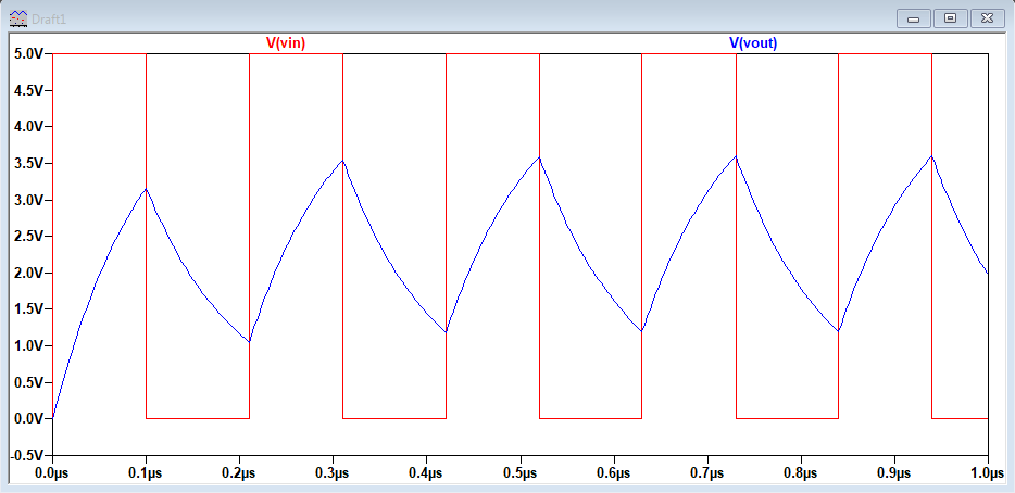
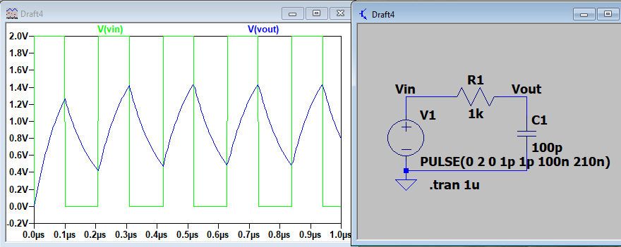
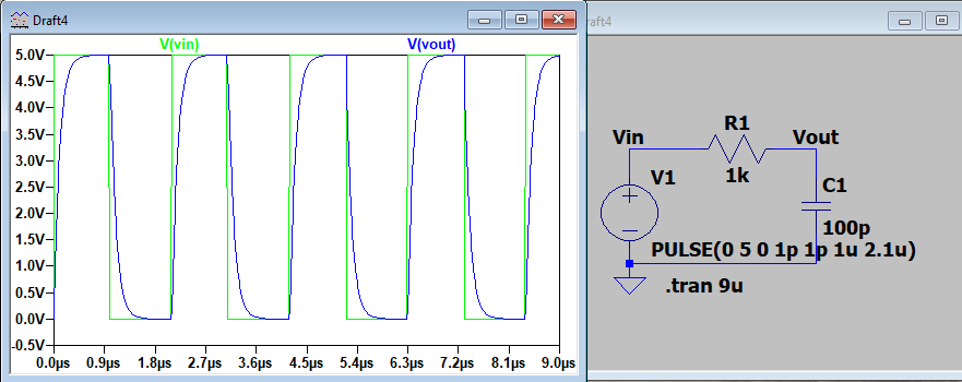
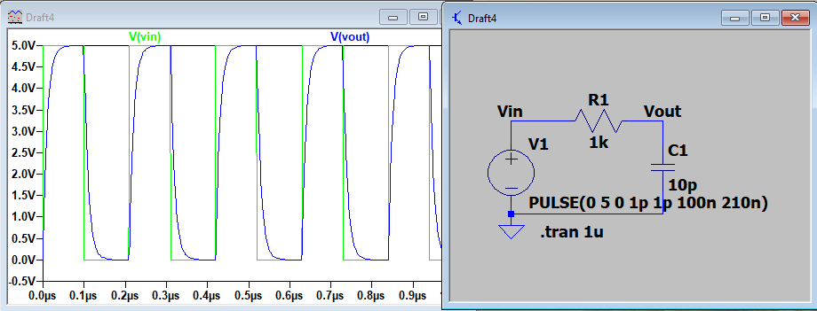
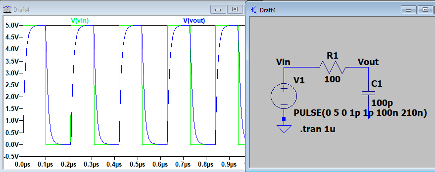
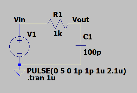
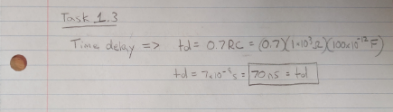
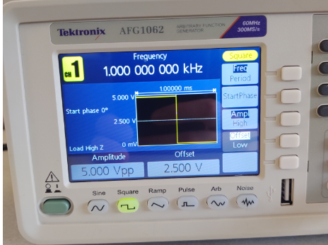
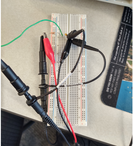
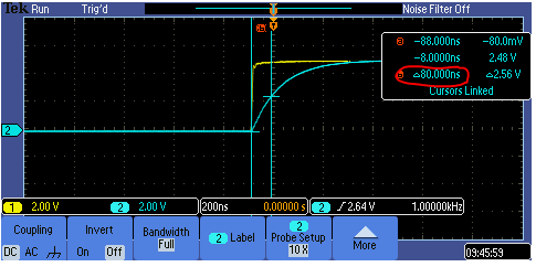
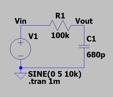
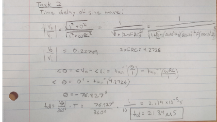
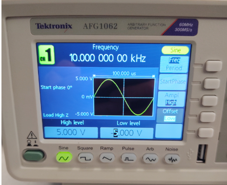
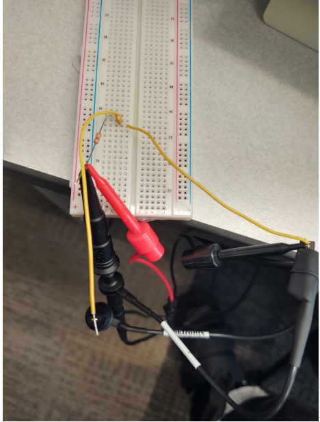
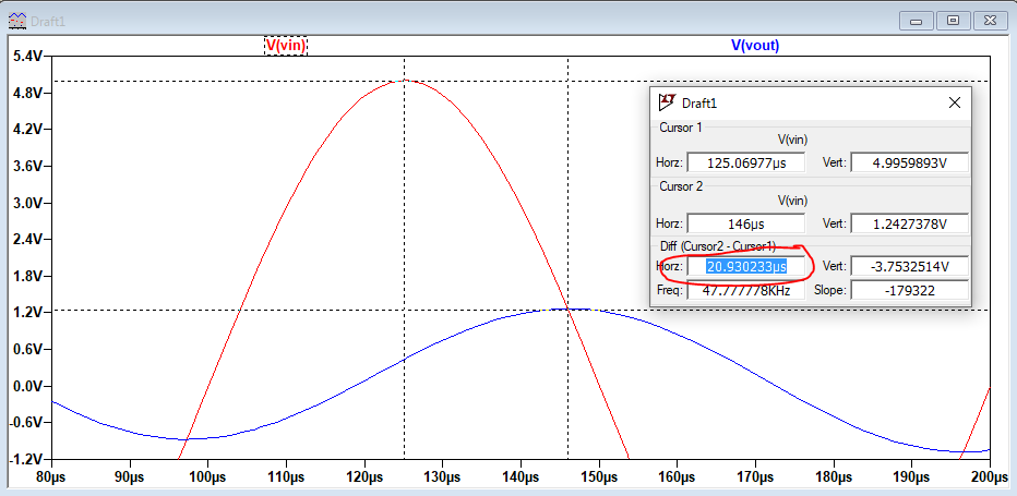
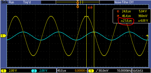
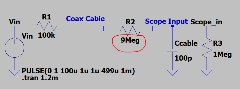
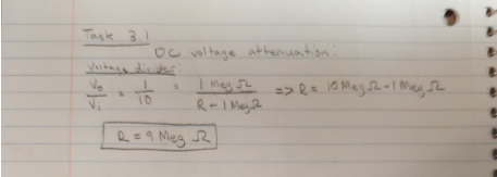
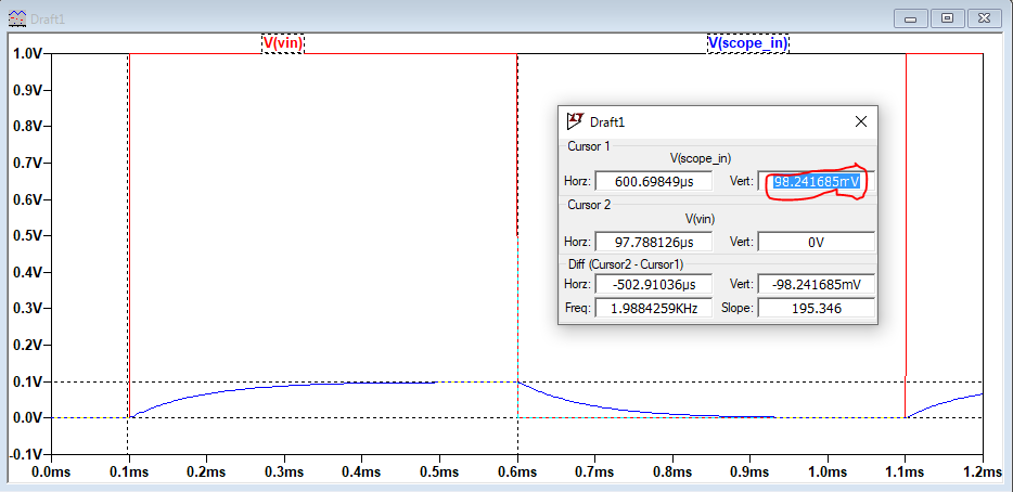
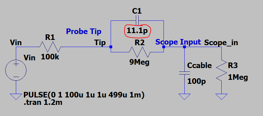
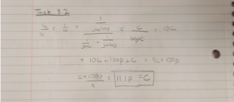
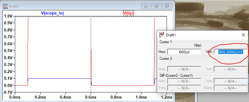
Task 1.1 had students create a circuit designed by Dr. Li in LTSpice and simulate it. The students then had to alter the circuit slightly in Task 1.2, parts a through d, and explain if their modifications helped the capacitor in the RC circuit reach full charge or did not allow it to reach full charge. These changes included altering the input signal voltage, changinge the capcaitance, changing the resistor, and changing the period of the input signal. These changes can been seen in the Results section of the report. Students then used a bread board to construct an RC circuit using the materials above and send both a sine and square wave to the circuit as an input signal in Task 1.3. The input and output voltages of the circuit was measured with an oscilliscope for both wave types and recorded. In Task 2, students calculated and simulated the time delay of an sine wave input to an RC circuit as well as the amplitude attentuation of the circuit. The circuit was also contructed on a bread board and the results were measured with the oscilliscope. In Task 3, students examined the internal circuit of a 10x compensated probe used by the oscilliscope and simulated its DC and AC attentuation in LTSpice. The correct resistance and capacitance had to be calculated in order to ensure the probe simulated with a 10x configuration.

4. Results


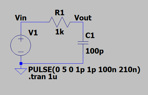
Figure 1. The RC circuit used in Task 1.1 with labeled voltage nodes and currents provided by Dr. Li.


Figure 2. The simulation of the circuit displayed graphically. The capacitor in this circuit cannot be fully charged to the 5V volatage range because there is insuffcient bandwidth in the circuit. The frequency is too high and does not allow for sufficient charging time.


Figure 3. The altered circuit from Task 1 for Task 1.2 a) and its simulation. Notice the input voltage has been dropped to 2V and yet the capacitor cannot reach its full charge. This is still the case because the bandwidth is still insufficient for charging the capacitor to full charge for the given frequency.


Figure 4. The altered circuit and simulation for Task 1.2 b). The frequency has been lowered in this configuration and the capacitor can no2 reach its full charge. This is because the bandwidth now has time to fully incorperate the input signal of the circuit.


Figure 5. The circuit and simulation for Task 1.2 c).
The capacitor charges fully in this configuration very rapidly because its capacitance has been reduced by a factor of 10.


Figure 6. The circuit and simulation for Task 1.2 d).
Decreasing the resistance within the circuit also allows the capacitor to reach full charge because this allows more current to flow through the circuit charging up the capacitor more quickly than in the first configuration.


Figure 7. The ciruit used for simulation in Task 1.3.


Figure 8. The time delay calculation used for the circuit with a square wave input signal.


Figure 9. The function generator square wave input signal.


Figure 10. The bread board setup for the circuit from Task 1.3.


Figure 11. The oscilliscope reading for the Task 1.3 circuit showing the time delay.


Figure 12. The circuit for Task 2.


Figure 13. The calculations for the time delay and amplitutde attentuation for Task 2.


Figure 14. The function generator sine wave input signal.


Figure 15. The Task 2 circuit constructed on the bread board.


Figure 16. The simulated time delay and amplituted attentuation for Task 2 in LTSpice.


Figure 17. The oscilliscope reading for the Task 2 circuit.

Table 1. The time delay and amplitude attentuation from each method of analyzation.

Hand Calculation
Oscilliscope Measurement
LTSpice Simulation
Vin 5 V 5.04 V 5 V
Vout 1.139 V 0.960 V 1.243 V
Vin/Vout 0.22789 0.1905 0.2486
Time Delay
21.34 uS 21.6 uS
20.93 uS


Figure 18. The circuit used to represent the DC compensated probe from Task 3.1. The circled resistance was calculated assuming the probe had a compensation for 10x.


Figure 19. The hand calcuations done to find the resistance needed to create a 10x compensated probe.


Figure 20. The LTSpice simulaiton showing the 10x attenuation of the compensated probe while measuring DC signal.


Figure 21. The circuit used to represent the AC 10x compensated probe. The circled capacitance is needed to ensure the probe has a 10x compensation.


Figure 22. The hand calculations done to find the needed capacitance.


Figure 23. The simulation showing the 10x attenuation of the AC signal for Task 3.2.

5. Discussion

Students continued to develop their LTSpice skills and knowledge during this lab as well as their understanding of RC circuits. The concept of the compensated probe further reinforced the ability of RC circuits to filter and alter input signals. The first tasks allowed students to see how variables such as frequency, time period, resistance, voltage, and capaciatance can change the ability of a capacitor to fully charge. Task 2 showed students how to properly use the oscilliscope and function generator and take measurements through the machines. The time delay for both Task 1.3 with a square wave input and Task 2 were very close to the calculated values even though the amplitutde attenuation values varied slightly. Task 3 highlighted how the parasitic capacitance and internal resistance of the compensated probe affects the attenuation of an measured signal in the oscilliscope. The concepts of time delay and amplitude attentuation were also reinforced and students continued to develop their math capabilities through the required hand calcualtions.

Task 3.3:
The 10x identifier is located on the probe input connection that attaches the probe to the oscilliscope. When the probe is set to a 1x configuration the output signal is not able to be displayed alongside the input signal. This is because the ouput amplitude is much smaller than the input amplitude. For example, when tested with an input signal of 5 volts the output signal was measured to be around 150 milivolts. When the signal is in the 10x configuration both signals can be seen clearly next to each on the oscilliscope screen.