1. Op Amp IC with ESD Protection Completion (Final Project) 2. In this lab, students completed the final design for their
analog integrated circuits with ESD protection. This lab served as the
culmination for student learning within the lab portion of the class
and a final demonstration of the concepts of analog circuit design
practiced in ElectricVLSI. This covered the information found in
Tutorial 5 and was the final lab completed for the semester. A
completed Op Amp was designed and placed in the ESD pad frame
constructed by students in Tutorial 4. A capacitor was also completed
and wired to the Op Amp. The inverter designed by students earlier on
in the semester was also incorperated into this final project.
3. Materials
LTSpice
software (for simulation)
ElectricVLSI Software
Java (for running ElectricVLSI)
Methods Students
began the lab by designing the final Op Amp in LTSpice. Students
simulated the open loop gain for the Op Amp and demtermined the
resistance a resistor within the Op Amp had to hold in order to keep
all DC operating points within their saturation regions. Students
captured screenshots of the open loop gain. ElectricVLSI was then
opened and students followed an instructional video posted by Dr. Li
describing how to design the biasing circuit required for the Op Amp
design. Students created three PMOS and three NMOS MOSFET's and wired
them according to the design described in the video. The MOSFET's were
properly sized and wired to their required N or P wells. A layout,
schematic, and icon were created of the biasing circuit and students
conducted DRC and NCC checks to ensure the design was correct. The gain
stage and differential pairs of the Op Amp were designed in a second
instructional video. Students had to create large NMOS and PMOS
MOSFET's by stacking smaller ones on top of each other. These MOSFET's
were wired together to create the larger ones needed for the Op Amp.
Upon completion, they were wired to the ground and vdd terminals. The
pins were wired to the ports needed for completing the final circuit.
Metal one and two wires were used to ensure the design did not conflict
with itself. Another round of DRC and NCC checks were compeleted
to make sure this time consuming part of the lab was completed
correctly. After the circuit proved correct the biasing circuit was connected to the differential pairs and gain stage of the Op Amp.
Students then followed along with the third and final video posted by
Dr. Li and constructed a 10 pF capcitor for use with the Op Amp. The
capacitor had to have an area of 130,000 relative to the pad frame.
Once the capacitor was completed, it was wired to the Op Amp. Pins 36
through 5 were exported on the ESD pad frame for use in wiring the Op
Amp and inverter. The pad frame pins were wired to both the Op Amp and
inverter pins. The pad frame schematic was wired with the Op Amp and
inverter icons in the same manner as the layout. The final DRC and NCC
checks were conducted on the completed analog IC and the final project
was finished when the checks came back correct. Screenshots of all the
IC components as well as the DRC and NCC checks were captured for the
final report. The completed VLSI file was saved as tutorial_5.jleb.
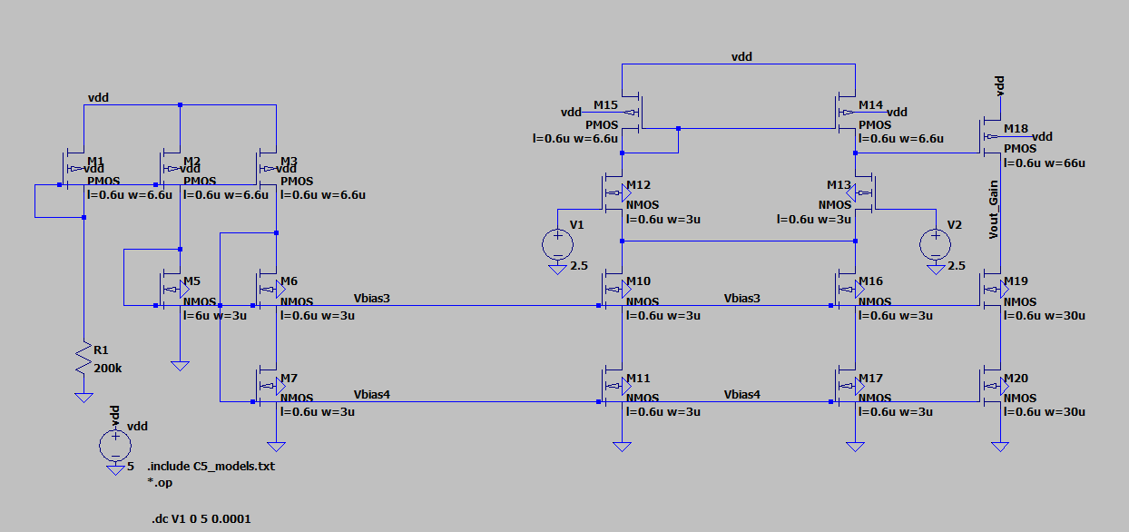
4. Results Figure 1. The
completed LTSpice Op Amp circuit used to simulate the open loop gain.
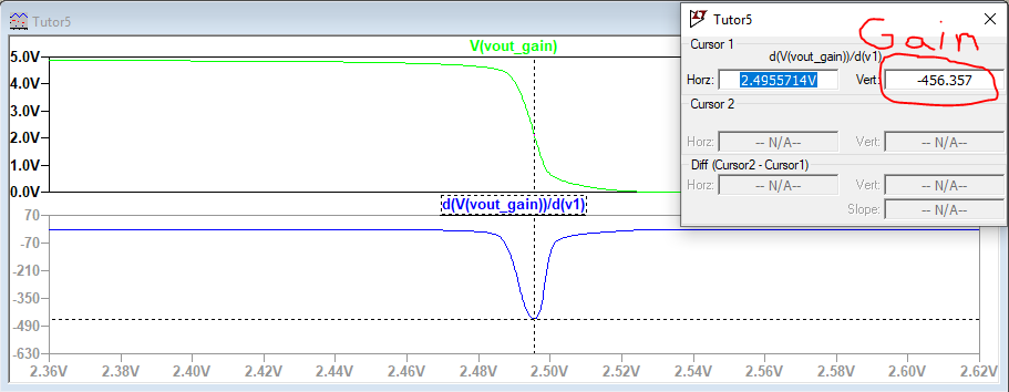
Figure 2. The
simulated open loop gain for the Op Amp with a 200k ohm resistor used
to keep the DC operating points in their saturation regions.
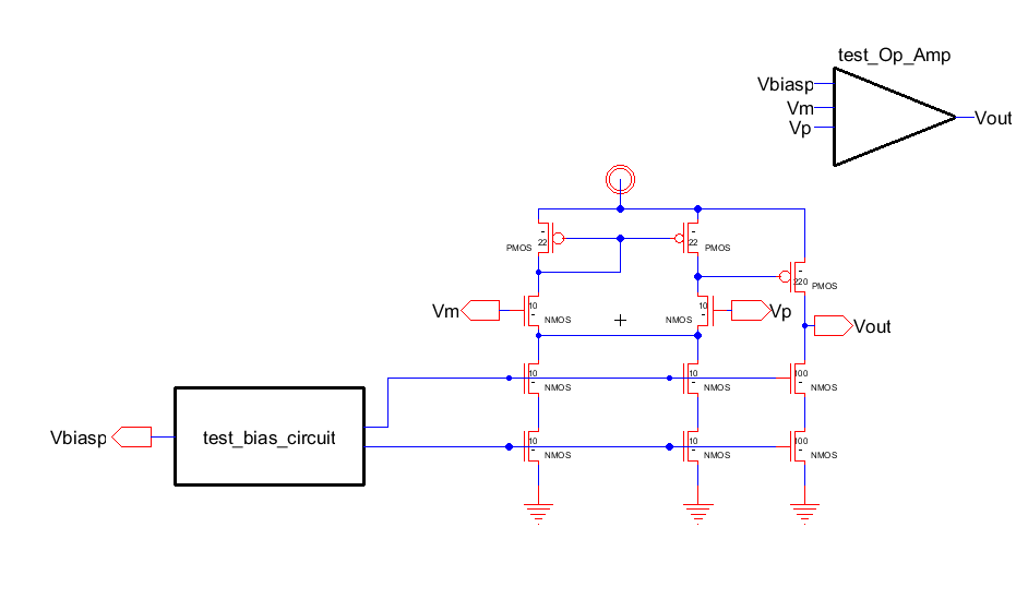
Figure 3. The
completed ElectricVLSI schematic and icon for the biasing circuit as specified in the first video (provided by Dr. Li).
Figure 4. The
completed layout for the biasing circuit as specified in the first video (provided by Dr. Li).
Figure 5. The
completed schematic and icon for the Op Amp with biasing circuit as specified in the second video (provided by Dr. Li).
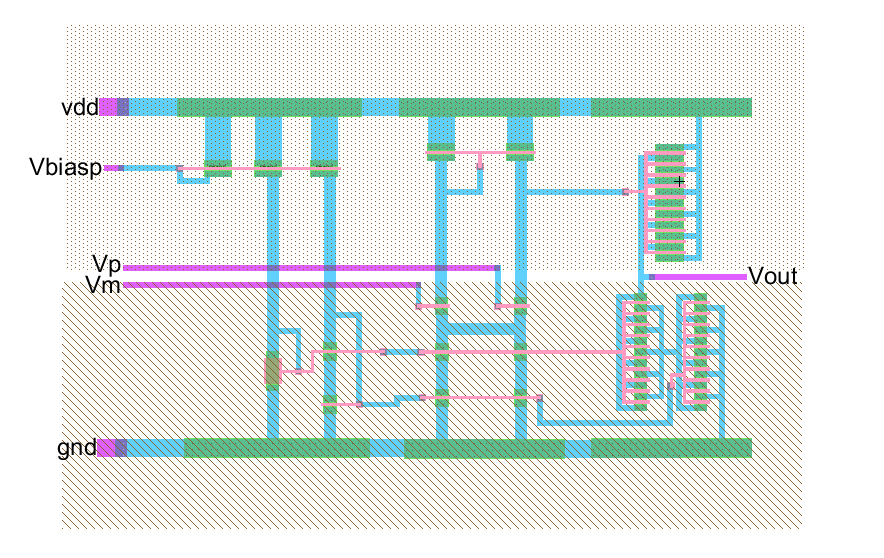
Figure 6. The
completed layout for the Op Amp with biasing circuit as specified in the second video (provided by Dr. Li).
Figure 7. The
completed DRC and NCC checks for the Op Amp with biasing circuit. Both checks revealed the circuit was error free. Figure 8. The
completed schematic for the 10 pF capacitor wired to the Op Amp as specified in the third video (provided by Dr. Li).
Figure 9. The
completed layout for the 10 pF capacitor wired to the Op Amp as specified in the third video (provided by Dr. Li).
Figure 10. The
completed schematic for the final project IC chip as specified in the third video (provided by Dr. Li).
Figure 11. The
completed layout for the final project IC chip as specified in the third video (provided by Dr. Li). The Op Amp, capacitor, and inverter can all be seen.
Figure 12. The completed DRC and NCC checks the final project IC chip as specified in the third video (provided by Dr. Li). Both checks revealed the circuit was error free.
5. Discussion This
lab was the fifth and final lab of the ElectricVLSI lab series.
Tutorial Five served as the culmination of student learning for the lab
portion of the class and had students demonstrate the necessary skills
used in analog circuit design. Students also demonstrated the skills
they learned in the ElectricVLSI program. Students incorperated all the
circuit components completed in previous labs into their final project
IC chips. The process proved time consuiming and painful. Numerous
errors and setback were encountered and restarting protions of the lab
was sometimes necessary. The NRC errors proved especially difficult to
work through as they often required careful examination of the entire
circuit. Exporting the pins on the ESD pad frame was very tedious as
well. It is a wonder why no one has created a means for the VLSI
program to perform that process automatically. Despite the setbacks and
lost time, students were able to complete their circuits free of
errors. The videos posted by Dr. Li were invaluable and the lab would
have been almost impossible to complete without them. The experience
and knowledge gained from completing an analog IC chips proved
extremely valueable. The job of an analog engineer was experienced
throughout these tutorials and the content taught by Dr. Li in the
lectures proved both practical and useful. It was made clear why not
many people choose to pursue a career in analog circuits as desiging
these circuits can be difficult and tedious. However, the neccesity of
the profession was also made apparent. Many
technolgies used today
incorpeate analog circuits and students experienced a small taste of
how much time and effort must go into designing these circuits. The
ElectricVLSI lab series served as an excellent way to test student
learning from the entire course. The final project was both challenging
and rewarding and an extremely useful experience for students moving
forward in their educations and careers.